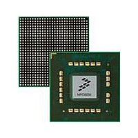
MPC8536DS Freescale Semiconductor, MPC8536DS Datasheet - Page 662

MPC8536DS
Manufacturer Part Number
MPC8536DS
Description
BOARD DEV SYSTEM MPC8536E
Manufacturer
Freescale Semiconductor
Series
PowerQUICC III™r
Type
MPUr
Datasheets
1.MPC8536EBVTAVLA.pdf
(127 pages)
2.MPC8536EBVTAVLA.pdf
(1706 pages)
3.MPC8536DS.pdf
(2 pages)
4.MPC8536DS.pdf
(126 pages)
Specifications of MPC8536DS
Contents
Board, Software and Documentation
Processor Series
MPC85xx
Core
e500
Data Bus Width
32 bit
Maximum Clock Frequency
667 MHz
Operating Supply Voltage
- 0.3 V to + 1.21 V
Maximum Operating Temperature
+ 105 C
Data Ram Size
32 KB
Interface Type
SPI, USB
Program Memory Type
DDR2, DDR3, SDRAM
Core Size
32 Bit
Program Memory Size
544KB
Cpu Speed
1.5GHz
Digital Ic Case Style
BGA
No. Of Pins
783
Supply Voltage Range
0.95V To 1.05V
Rohs Compliant
Yes
For Use With/related Products
MPC8536
Lead Free Status / RoHS Status
Lead free / RoHS Compliant
- MPC8536EBVTAVLA PDF datasheet
- MPC8536EBVTAVLA PDF datasheet #2
- MPC8536DS PDF datasheet #3
- MPC8536DS PDF datasheet #4
- Current page: 662 of 1706
- Download datasheet (15Mb)
Enhanced Local Bus Controller
Table 13-9
13.3.1.3
Figure 13-6
13-20
17–18
20–22
24–28
0–16
Offset 0x0_5068
Bits
Reset
19
23
29
30
31
W
R
BCTLD Buffer control disable. Disables assertion of LBCTL during access to the current memory bank.
0
Name
EHTR Extended hold time on read accesses. Indicates with TRLX how many cycles are inserted between a read
TRLX
EAD
AM
—
—
—
BI
describes BRn fields for UPM mode.
shows the fields of the UPM memory address register (MAR).
UPM Memory Address Register (MAR)
UPM address mask. Masks corresponding BR n bits. Masking address bits independently allows external
devices of different size address ranges to be used. Address mask bits can be set or cleared in any order in
the field, allowing a resource to reside in more than one area of the address map.
0 Corresponding address bits are masked.
1 The corresponding address bits are used in the comparison with address pins.
Reserved
0 LBCTL is asserted upon access to the current memory bank.
1 LBCTL is not asserted upon access to the current memory bank.
Reserved
Burst inhibit. Indicates if this memory bank supports burst accesses.
0 The bank supports burst accesses.
1 The bank does not support burst accesses. The selected UPM executes burst accesses as a series of
Reserved
Timing relaxed. Works in conjunction with EHTR to extend hold time on read accesses.
access from the current bank and the next access.
External address latch delay. Allow extra bus clock cycles when using external address latch (LALE).
0 No additional bus clock cycles (LALE asserted for one bus clock cycle only)
1 Extra bus clock cycles are added (LALE is asserted for the number of bus clock cycles specified by
single accesses.
LCRR[EADC]).
TRLX EHTR
MPC8536E PowerQUICC III Integrated Processor Reference Manual, Rev. 1
0
0
1
1
0
1
0
1
Figure 13-6. UPM Memory Address Register (MAR)
The memory controller generates normal timing. No additional cycles are inserted.
1 idle clock cycle is inserted.
4 idle clock cycles are inserted.
8 idle clock cycles are inserted.
Table 13-9. OR n
—
UPM Field Descriptions
All zeros
Description
A
Meaning
Freescale Semiconductor
Access: Read/Write
31
Related parts for MPC8536DS
Image
Part Number
Description
Manufacturer
Datasheet
Request
R
Part Number:
Description:
Manufacturer:
Freescale Semiconductor, Inc
Datasheet:
Part Number:
Description:
Manufacturer:
Freescale Semiconductor, Inc
Datasheet:
Part Number:
Description:
Manufacturer:
Freescale Semiconductor, Inc
Datasheet:
Part Number:
Description:
Manufacturer:
Freescale Semiconductor, Inc
Datasheet:
Part Number:
Description:
Manufacturer:
Freescale Semiconductor, Inc
Datasheet:
Part Number:
Description:
Manufacturer:
Freescale Semiconductor, Inc
Datasheet:
Part Number:
Description:
Manufacturer:
Freescale Semiconductor, Inc
Datasheet:
Part Number:
Description:
Manufacturer:
Freescale Semiconductor, Inc
Datasheet:
Part Number:
Description:
Manufacturer:
Freescale Semiconductor, Inc
Datasheet:
Part Number:
Description:
Manufacturer:
Freescale Semiconductor, Inc
Datasheet:
Part Number:
Description:
Manufacturer:
Freescale Semiconductor, Inc
Datasheet:
Part Number:
Description:
Manufacturer:
Freescale Semiconductor, Inc
Datasheet:
Part Number:
Description:
Manufacturer:
Freescale Semiconductor, Inc
Datasheet:
Part Number:
Description:
Manufacturer:
Freescale Semiconductor, Inc
Datasheet:
Part Number:
Description:
Manufacturer:
Freescale Semiconductor, Inc
Datasheet:


