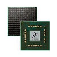
MPC8536DS Freescale Semiconductor, MPC8536DS Datasheet - Page 866

MPC8536DS
Manufacturer Part Number
MPC8536DS
Description
BOARD DEV SYSTEM MPC8536E
Manufacturer
Freescale Semiconductor
Series
PowerQUICC III™r
Type
MPUr
Datasheets
1.MPC8536EBVTAVLA.pdf
(127 pages)
2.MPC8536EBVTAVLA.pdf
(1706 pages)
3.MPC8536DS.pdf
(2 pages)
4.MPC8536DS.pdf
(126 pages)
Specifications of MPC8536DS
Contents
Board, Software and Documentation
Processor Series
MPC85xx
Core
e500
Data Bus Width
32 bit
Maximum Clock Frequency
667 MHz
Operating Supply Voltage
- 0.3 V to + 1.21 V
Maximum Operating Temperature
+ 105 C
Data Ram Size
32 KB
Interface Type
SPI, USB
Program Memory Type
DDR2, DDR3, SDRAM
Core Size
32 Bit
Program Memory Size
544KB
Cpu Speed
1.5GHz
Digital Ic Case Style
BGA
No. Of Pins
783
Supply Voltage Range
0.95V To 1.05V
Rohs Compliant
Yes
For Use With/related Products
MPC8536
Lead Free Status / RoHS Status
Lead free / RoHS Compliant
- MPC8536EBVTAVLA PDF datasheet
- MPC8536EBVTAVLA PDF datasheet #2
- MPC8536DS PDF datasheet #3
- MPC8536DS PDF datasheet #4
- Current page: 866 of 1706
- Download datasheet (15Mb)
Enhanced Three-Speed Ethernet Controllers
14.5.3.9
This section describes the two eTSEC DMA attribute registers.
14.5.3.9.1
The attribute register defines memory access attributes and transaction types used to access buffer
descriptors, to write receive data, and to read transmit data. Snoop enable attributes may be set for reading
buffer descriptors and for reading transmit data. Buffer descriptors may be written with attributes that
cause allocation into the L2 cache. Similarly, broad sections of a receive frame header may have attributes
attached that cause allocation in the L2 cache. This process of specifying a region of each frame to stash
into the L2 cache is referred to as extraction, which is specified in conjunction with register ATTRELI.
ATTR[ELCWT] only has meaning if ATTRELI[EL] is non-zero. It is important to note that even though
portions of received frames may be stashed to L2 cache, this is only a performance optimization as entire
frames are still written to off-chip memory regardless of settings in ATTR.
Figure 14-106
14-118
30–31
Bits
26
27
28
29
Offset eTSEC1:0x2_4BF8;
Reset
W
R
CRCAPP Append a CRC (CRC-32 algorithm, as per IEEE Std. 802.3) to the end of every transmitted frame.
CRCCHK Check the CRC (CRC-32 algorithm, as per IEEE Std. 802.3) at the end of every frame.
eTSEC3:0x2_6BF8
0
Name
SIGM
FFC
—
DMA Attribute Registers
describes the definition for the ATTR register.
Attribute Register (ATTR)
Force flow control. This can be used by software to stop reception on the FIFO interface.
0 Do not assert link-level flow control through the RXFC signal unless eTSEC requires flow control.
1 Force flow control on the RXFC signal in encoded FIFO packet mode regardless of eTSEC pause
0 Do not automatically append a CRC to transmitted frames. Allow TxBD[TC], if set, to control when a
1 Automatically append a CRC to transmitted frames. Ignore TxBD[TC].
0 Do not automatically check the last 4 bytes of received frames for a valid CRC.
1 Automatically check the last 4 bytes of received frames for a valid CRC. If a CRC error is detected, or
Reserved
FIFO signaling mode. Determines how the GMII signals are interpreted as framing signals.
00 GMII style mode.
01 Encoded packet mode.
10 Reserved
11 Reserved
requirements.
CRC is appended.
insufficient data is received to recover the CRC, the RxBD[CR] bit is set.
MPC8536E PowerQUICC III Integrated Processor Reference Manual, Rev. 1
Table 14-109. FIFOCFG Field Descriptions (continued)
—
Figure 14-106. ATTR Register Definition
16
ELCWT
17
18
All zeros
—
19
Description
BDLWT
20
21
22 23
—
RDSEN RBDSEN
24
25
Freescale Semiconductor
Access: Read/Write
26
—
31
Related parts for MPC8536DS
Image
Part Number
Description
Manufacturer
Datasheet
Request
R
Part Number:
Description:
Manufacturer:
Freescale Semiconductor, Inc
Datasheet:
Part Number:
Description:
Manufacturer:
Freescale Semiconductor, Inc
Datasheet:
Part Number:
Description:
Manufacturer:
Freescale Semiconductor, Inc
Datasheet:
Part Number:
Description:
Manufacturer:
Freescale Semiconductor, Inc
Datasheet:
Part Number:
Description:
Manufacturer:
Freescale Semiconductor, Inc
Datasheet:
Part Number:
Description:
Manufacturer:
Freescale Semiconductor, Inc
Datasheet:
Part Number:
Description:
Manufacturer:
Freescale Semiconductor, Inc
Datasheet:
Part Number:
Description:
Manufacturer:
Freescale Semiconductor, Inc
Datasheet:
Part Number:
Description:
Manufacturer:
Freescale Semiconductor, Inc
Datasheet:
Part Number:
Description:
Manufacturer:
Freescale Semiconductor, Inc
Datasheet:
Part Number:
Description:
Manufacturer:
Freescale Semiconductor, Inc
Datasheet:
Part Number:
Description:
Manufacturer:
Freescale Semiconductor, Inc
Datasheet:
Part Number:
Description:
Manufacturer:
Freescale Semiconductor, Inc
Datasheet:
Part Number:
Description:
Manufacturer:
Freescale Semiconductor, Inc
Datasheet:
Part Number:
Description:
Manufacturer:
Freescale Semiconductor, Inc
Datasheet:


