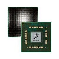
MPC8536DS Freescale Semiconductor, MPC8536DS Datasheet - Page 703

MPC8536DS
Manufacturer Part Number
MPC8536DS
Description
BOARD DEV SYSTEM MPC8536E
Manufacturer
Freescale Semiconductor
Series
PowerQUICC III™r
Type
MPUr
Datasheets
1.MPC8536EBVTAVLA.pdf
(127 pages)
2.MPC8536EBVTAVLA.pdf
(1706 pages)
3.MPC8536DS.pdf
(2 pages)
4.MPC8536DS.pdf
(126 pages)
Specifications of MPC8536DS
Contents
Board, Software and Documentation
Processor Series
MPC85xx
Core
e500
Data Bus Width
32 bit
Maximum Clock Frequency
667 MHz
Operating Supply Voltage
- 0.3 V to + 1.21 V
Maximum Operating Temperature
+ 105 C
Data Ram Size
32 KB
Interface Type
SPI, USB
Program Memory Type
DDR2, DDR3, SDRAM
Core Size
32 Bit
Program Memory Size
544KB
Cpu Speed
1.5GHz
Digital Ic Case Style
BGA
No. Of Pins
783
Supply Voltage Range
0.95V To 1.05V
Rohs Compliant
Yes
For Use With/related Products
MPC8536
Lead Free Status / RoHS Status
Lead free / RoHS Compliant
- MPC8536EBVTAVLA PDF datasheet
- MPC8536EBVTAVLA PDF datasheet #2
- MPC8536DS PDF datasheet #3
- MPC8536DS PDF datasheet #4
- Current page: 703 of 1706
- Download datasheet (15Mb)
Enhanced Local Bus Controller
Following the assertion of LALE, FCM asserts LCSn to commence a command sequence to the Flash
device. After a delay of t
, the first command can be written to the device on assertion of LFWE,
CSCT
followed by any parameters (typically address bytes and data), and concluded with a secondary command.
In many cases, the second command initiates a long-running operation inside the Flash device, which pulls
the wired-OR pin LFRB low to indicate that the device is busy. Since in
Figure 13-47
FCM is now
expecting a read response, it takes LBCTL low to turnaround any bus transceivers that are present. Upon
LFRB indicating ready status, FCM asserts LFRE repeatedly to recover bytes of read data, and the bytes
are stored in eLBC’s FCM buffer RAM while an ECC is optionally computed on the bytes transferred.
Finally, FCM negates LCSn and delays eLBC by t
before any subsequent memory access occurs.
EHTR
13.4.3.1
FCM Buffer RAM
Read and write accesses to eLBC banks controlled by FCM do not access attached NAND Flash
EEPROMs directly. Rather, these accesses read and write the FCM buffer RAM—a single, shared 8-Kbyte
space internal to eLBC and mapped by the base address of every FCM bank. Even though each
FCM-controlled bank will have a different base address to differentiate it, all accesses to such banks will
access the same buffer space. External eLBC signals, such as LALE and LCSn, will not assert upon
accesses to the buffer RAM. The FCM buffer RAM is logically divided into two or more buffers,
depending on the setting of ORn[PGS], with different buffers being accessible concurrently by software
and FCM.
To perform a page read operation from a NAND Flash device, software initializes the FCM command,
mode, and address registers, before issuing a special operation (FMR[OP] set non-zero) to a particular
FCM-controlled bank. FCM will execute the sequence of op-codes held in FIR, reading data from the
Flash device into the shared buffer RAM. While this read is taking place, software is free to access any
data stored in other, currently inactive buffers of the FCM buffer RAM through reads or writes to any bank
controlled by FCM. If command completion interrupts are enabled, an interrupt will be generated once
FCM has completed the read. When FCM has completed its last command, software can switch to the
newly read buffer and issue further commands.
To perform a page write operation, software first prepares data to be written in a fresh buffer. Then, the
FCM command, mode, and address registers are initialized, and a special operation (FMR[OP] set
non-zero) is issued to a particular FCM-controlled bank. FCM will execute the sequence of op-codes held
in FIR, writing data from shared buffer RAM to the Flash device. To ensure that the device is enabled for
programming, software must initialize FMR[OP] = 11, which prevents assertion of LFWP during the
write. While this write is taking place, software is free to access any data stored in other, currently inactive
buffers of the FCM buffer RAM through reads or writes to any bank controlled by FCM. When FCM has
completed its last command, software can re-use the previously written buffer and issue further
commands.
See
Section 13.4.3.4.2, “Boot Block Loading into the FCM Buffer RAM,”
for a description of the shared
buffer RAM layout during boot.
13.4.3.1.1
Buffer Layout and Page Mapping for Small-Page NAND Flash Devices
The FCM buffer space is divided into eight 1-Kbyte buffers for small-page devices (ORn[PGS] = 0),
mapped as shown in
Figure
13-48. Each page in a small-page NAND Flash comprises 528 bytes, where
MPC8536E PowerQUICC III Integrated Processor Reference Manual, Rev. 1
Freescale Semiconductor
13-61
Related parts for MPC8536DS
Image
Part Number
Description
Manufacturer
Datasheet
Request
R
Part Number:
Description:
Manufacturer:
Freescale Semiconductor, Inc
Datasheet:
Part Number:
Description:
Manufacturer:
Freescale Semiconductor, Inc
Datasheet:
Part Number:
Description:
Manufacturer:
Freescale Semiconductor, Inc
Datasheet:
Part Number:
Description:
Manufacturer:
Freescale Semiconductor, Inc
Datasheet:
Part Number:
Description:
Manufacturer:
Freescale Semiconductor, Inc
Datasheet:
Part Number:
Description:
Manufacturer:
Freescale Semiconductor, Inc
Datasheet:
Part Number:
Description:
Manufacturer:
Freescale Semiconductor, Inc
Datasheet:
Part Number:
Description:
Manufacturer:
Freescale Semiconductor, Inc
Datasheet:
Part Number:
Description:
Manufacturer:
Freescale Semiconductor, Inc
Datasheet:
Part Number:
Description:
Manufacturer:
Freescale Semiconductor, Inc
Datasheet:
Part Number:
Description:
Manufacturer:
Freescale Semiconductor, Inc
Datasheet:
Part Number:
Description:
Manufacturer:
Freescale Semiconductor, Inc
Datasheet:
Part Number:
Description:
Manufacturer:
Freescale Semiconductor, Inc
Datasheet:
Part Number:
Description:
Manufacturer:
Freescale Semiconductor, Inc
Datasheet:
Part Number:
Description:
Manufacturer:
Freescale Semiconductor, Inc
Datasheet:


