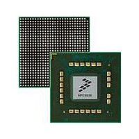
MPC8536DS Freescale Semiconductor, MPC8536DS Datasheet - Page 664

MPC8536DS
Manufacturer Part Number
MPC8536DS
Description
BOARD DEV SYSTEM MPC8536E
Manufacturer
Freescale Semiconductor
Series
PowerQUICC III™r
Type
MPUr
Datasheets
1.MPC8536EBVTAVLA.pdf
(127 pages)
2.MPC8536EBVTAVLA.pdf
(1706 pages)
3.MPC8536DS.pdf
(2 pages)
4.MPC8536DS.pdf
(126 pages)
Specifications of MPC8536DS
Contents
Board, Software and Documentation
Processor Series
MPC85xx
Core
e500
Data Bus Width
32 bit
Maximum Clock Frequency
667 MHz
Operating Supply Voltage
- 0.3 V to + 1.21 V
Maximum Operating Temperature
+ 105 C
Data Ram Size
32 KB
Interface Type
SPI, USB
Program Memory Type
DDR2, DDR3, SDRAM
Core Size
32 Bit
Program Memory Size
544KB
Cpu Speed
1.5GHz
Digital Ic Case Style
BGA
No. Of Pins
783
Supply Voltage Range
0.95V To 1.05V
Rohs Compliant
Yes
For Use With/related Products
MPC8536
Lead Free Status / RoHS Status
Lead free / RoHS Compliant
- MPC8536EBVTAVLA PDF datasheet
- MPC8536EBVTAVLA PDF datasheet #2
- MPC8536DS PDF datasheet #3
- MPC8536DS PDF datasheet #4
- Current page: 664 of 1706
- Download datasheet (15Mb)
Enhanced Local Bus Controller
13-22
10–12
14–17
Bits
5–7
8–9
13
Name
G0CL General line 0 control. Determines which logical address line can be output to the LGPL0 pin when the UPM n
GPL4
RLF
AM
DS
Address multiplex size. Determines how the address of the current memory cycle can be output on the
address pins. This field is needed when interfacing with devices requiring row and column addresses
multiplexed on the same pins. See
000 Internal transaction address a[8:23] driven on LAD[16:31]; LAD[0:15] driven low.
001 Internal transaction address a[7:22] driven on LAD[16:31]; LAD[0:15] driven low.
010 Internal transaction address a[6:21] driven on LAD[16:31]; LAD[0:15] driven low.
011 Internal transaction address a[5:20] driven on LAD[16:31]; LAD[0:15] driven low.
100 Internal transaction address a[4:19] driven on LAD[16:31]; LAD[0:15] driven low.
101 Internal transaction address a[3:18] driven on LAD[16:31]; LAD[0:15] driven low.
110 Reserved
111 Reserved
Disable timer period. Guarantees a minimum time between accesses to the same memory bank controlled
by UPM n . The disable timer is turned on by the TODT bit in the RAM array word, and when expired, the UPM n
allows the machine access to handle a memory pattern to the same bank. Accesses to a different bank by
the same UPM n is also allowed. To avoid conflicts between successive accesses to different banks, the
minimum pattern in the RAM array for a request serviced, should not be shorter than the period established
by DS.
00 1-bus clock cycle disable period
01 2-bus clock cycle disable period
10 3-bus clock cycle disable period
11 4-bus clock cycle disable period
is selected to control the memory access.
000 A12
001 A11
010 A10
011 A9
100 A8
101 A7
110 A6
111 A5
LGPL4 output line disable. Determines how the LGPL4/LUPWAIT pin is controlled by the corresponding bits
in the UPM n array. See
Read loop field. Determines the number of times a loop defined in the UPM n will be executed for a burst- or
single-beat read pattern or when M x MR[OP] = 11 (
0000 16
0001 1
0010 2
0011 3
...
1110 14
1111 15
MPC8536E PowerQUICC III Integrated Processor Reference Manual, Rev. 1
Value
0
1
Table 13-11. M x MR Field Descriptions (continued)
LGPL4/LUPWAIT
LUPWAIT (input)
LGPL4 (output)
Pin Function
Table 13-40 on page
Section 13.4.4.4.7, “Address Multiplexing
Interpretation of UPM Word Bits
G4T1/DLT3
13-81.
Description
G4T1
DLT3
RUN
command)
G4T3/WAEN
WAEN
G4T3
(AMX)” for more information.
Freescale Semiconductor
Related parts for MPC8536DS
Image
Part Number
Description
Manufacturer
Datasheet
Request
R
Part Number:
Description:
Manufacturer:
Freescale Semiconductor, Inc
Datasheet:
Part Number:
Description:
Manufacturer:
Freescale Semiconductor, Inc
Datasheet:
Part Number:
Description:
Manufacturer:
Freescale Semiconductor, Inc
Datasheet:
Part Number:
Description:
Manufacturer:
Freescale Semiconductor, Inc
Datasheet:
Part Number:
Description:
Manufacturer:
Freescale Semiconductor, Inc
Datasheet:
Part Number:
Description:
Manufacturer:
Freescale Semiconductor, Inc
Datasheet:
Part Number:
Description:
Manufacturer:
Freescale Semiconductor, Inc
Datasheet:
Part Number:
Description:
Manufacturer:
Freescale Semiconductor, Inc
Datasheet:
Part Number:
Description:
Manufacturer:
Freescale Semiconductor, Inc
Datasheet:
Part Number:
Description:
Manufacturer:
Freescale Semiconductor, Inc
Datasheet:
Part Number:
Description:
Manufacturer:
Freescale Semiconductor, Inc
Datasheet:
Part Number:
Description:
Manufacturer:
Freescale Semiconductor, Inc
Datasheet:
Part Number:
Description:
Manufacturer:
Freescale Semiconductor, Inc
Datasheet:
Part Number:
Description:
Manufacturer:
Freescale Semiconductor, Inc
Datasheet:
Part Number:
Description:
Manufacturer:
Freescale Semiconductor, Inc
Datasheet:


