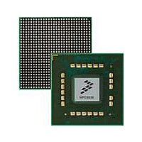
MPC8536DS Freescale Semiconductor, MPC8536DS Datasheet - Page 289

MPC8536DS
Manufacturer Part Number
MPC8536DS
Description
BOARD DEV SYSTEM MPC8536E
Manufacturer
Freescale Semiconductor
Series
PowerQUICC III™r
Type
MPUr
Datasheets
1.MPC8536EBVTAVLA.pdf
(127 pages)
2.MPC8536EBVTAVLA.pdf
(1706 pages)
3.MPC8536DS.pdf
(2 pages)
4.MPC8536DS.pdf
(126 pages)
Specifications of MPC8536DS
Contents
Board, Software and Documentation
Processor Series
MPC85xx
Core
e500
Data Bus Width
32 bit
Maximum Clock Frequency
667 MHz
Operating Supply Voltage
- 0.3 V to + 1.21 V
Maximum Operating Temperature
+ 105 C
Data Ram Size
32 KB
Interface Type
SPI, USB
Program Memory Type
DDR2, DDR3, SDRAM
Core Size
32 Bit
Program Memory Size
544KB
Cpu Speed
1.5GHz
Digital Ic Case Style
BGA
No. Of Pins
783
Supply Voltage Range
0.95V To 1.05V
Rohs Compliant
Yes
For Use With/related Products
MPC8536
Lead Free Status / RoHS Status
Lead free / RoHS Compliant
- MPC8536EBVTAVLA PDF datasheet
- MPC8536EBVTAVLA PDF datasheet #2
- MPC8536DS PDF datasheet #3
- MPC8536DS PDF datasheet #4
- Current page: 289 of 1706
- Download datasheet (15Mb)
8.4.1.3
The chip select configuration (CSn_CONFIG_2) registers shown in
refresh address decode in each chip select.
If chip select interleaving is enabled, then all fields in the lower interleaved chip select are used, and the
other registers’ fields are unused.
Table 8-8
Freescale Semiconductor
24–28
29–31
Bits
Offset 0x0C0
Reset
8–31
Bits
0–4
5–7
W
R
0x0C4
0x0C8
0x0CC
0
COL_BITS_CS_ n
describes the CSn_CONFIG_2 register fields.
PASR_CFG
Chip Select Configuration 2 (CS n _CONFIG_2)
Name
—
Name
—
—
—
MPC8536E PowerQUICC III Integrated Processor Reference Manual, Rev. 1
Figure 8-4. Chip Select Configuration Register 2 (CS n _CONFIG_2)
4
PASR_CFG
5
Table 8-7. CS n _CONFIG Field Descriptions (continued)
Reserved
Partial array self refresh config. Controls the bits that are placed on MA[2:0] during the write to
the EMRS(2) register when the automatic hardware DRAM initialization is used
(DDR_SDRAM_CFG[BI] is cleared when DDR_SDRAM_CFG[MEM_EN] is set). If this field is
a non-zero value, then it overrides the least significant 3 bits in
DDR_SDRAM_MODE_2[ESDMODE2] during the automatic initialization for chip select n . In
addition, if a non-zero value is programmed in this field, then the address decode for chip select
n is optimized for partial array self refresh, as shown in
Multiplexing.
000 Partial array self refresh is disabled
001–111Partial array self refresh is enabled per JEDEC specifications. Overriding the least
Reserved
Reserved
Number of column bits for SDRAM on chip select n. For DDR, the decoding is as follows:
000 8 column bits
001 9 column bits
010 10 column bits
011 11 column bits
100–111 Reserved
significant 3 bits of EMRS or EMRS(2) is only supported for DDR2 and DDR3 memory
types.
Table 8-8. CS n _CONFIG_2 Field Descriptions
7
8
All zeros
Description
Description
Figure 8-4
—
Section 8.5.2, “DDR SDRAM Address
enable the partial array self
DDR Memory Controller
Access: Read/Write
31
8-15
Related parts for MPC8536DS
Image
Part Number
Description
Manufacturer
Datasheet
Request
R
Part Number:
Description:
Manufacturer:
Freescale Semiconductor, Inc
Datasheet:
Part Number:
Description:
Manufacturer:
Freescale Semiconductor, Inc
Datasheet:
Part Number:
Description:
Manufacturer:
Freescale Semiconductor, Inc
Datasheet:
Part Number:
Description:
Manufacturer:
Freescale Semiconductor, Inc
Datasheet:
Part Number:
Description:
Manufacturer:
Freescale Semiconductor, Inc
Datasheet:
Part Number:
Description:
Manufacturer:
Freescale Semiconductor, Inc
Datasheet:
Part Number:
Description:
Manufacturer:
Freescale Semiconductor, Inc
Datasheet:
Part Number:
Description:
Manufacturer:
Freescale Semiconductor, Inc
Datasheet:
Part Number:
Description:
Manufacturer:
Freescale Semiconductor, Inc
Datasheet:
Part Number:
Description:
Manufacturer:
Freescale Semiconductor, Inc
Datasheet:
Part Number:
Description:
Manufacturer:
Freescale Semiconductor, Inc
Datasheet:
Part Number:
Description:
Manufacturer:
Freescale Semiconductor, Inc
Datasheet:
Part Number:
Description:
Manufacturer:
Freescale Semiconductor, Inc
Datasheet:
Part Number:
Description:
Manufacturer:
Freescale Semiconductor, Inc
Datasheet:
Part Number:
Description:
Manufacturer:
Freescale Semiconductor, Inc
Datasheet:


