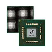
MPC8536DS Freescale Semiconductor, MPC8536DS Datasheet - Page 707

MPC8536DS
Manufacturer Part Number
MPC8536DS
Description
BOARD DEV SYSTEM MPC8536E
Manufacturer
Freescale Semiconductor
Series
PowerQUICC III™r
Type
MPUr
Datasheets
1.MPC8536EBVTAVLA.pdf
(127 pages)
2.MPC8536EBVTAVLA.pdf
(1706 pages)
3.MPC8536DS.pdf
(2 pages)
4.MPC8536DS.pdf
(126 pages)
Specifications of MPC8536DS
Contents
Board, Software and Documentation
Processor Series
MPC85xx
Core
e500
Data Bus Width
32 bit
Maximum Clock Frequency
667 MHz
Operating Supply Voltage
- 0.3 V to + 1.21 V
Maximum Operating Temperature
+ 105 C
Data Ram Size
32 KB
Interface Type
SPI, USB
Program Memory Type
DDR2, DDR3, SDRAM
Core Size
32 Bit
Program Memory Size
544KB
Cpu Speed
1.5GHz
Digital Ic Case Style
BGA
No. Of Pins
783
Supply Voltage Range
0.95V To 1.05V
Rohs Compliant
Yes
For Use With/related Products
MPC8536
Lead Free Status / RoHS Status
Lead free / RoHS Compliant
- MPC8536EBVTAVLA PDF datasheet
- MPC8536EBVTAVLA PDF datasheet #2
- MPC8536DS PDF datasheet #3
- MPC8536DS PDF datasheet #4
- Current page: 707 of 1706
- Download datasheet (15Mb)
13.4.3.2
FCM has a fully general command and data transfer sequencer that caters for both common and
specific/proprietary NAND Flash command sequences. The command sequencer reads a program out of
the FIR register, which can hold up to 8 instructions, each represented by a 4-bit op-code, as illustrated in
Figure
likewise to subsequent instructions, ending at FIR[OP7] or until the only instructions remaining are NOPs.
If FIR contains nothing but NOP instructions, FCM will not assert LCSn, otherwise, LCSn is asserted prior
to the first instruction and remains asserted until the last instruction has completed. If LTESR[CC] is
enabled, completion of the last instruction will trigger a command completion event interrupt from eLBC.
Prior to executing a sequence, necessary operands for the instructions will need to be set in the FMR, FCR,
MDR, FBCR, FBAR, and FPAR registers. The AS0–AS3 address and data pointers associated with FCM’s
use of MDR all reset to select AS0 at the start of the instruction sequence. A complete list of op-codes can
be found in
Freescale Semiconductor
ECCM
0
1
13-53. The first instruction executed is read from FIR[OP0], the next is read from FIR[OP1], and
Byte 0
Figure 13-52. ECC Placement in NAND Flash Spare Regions in Relation to FMR[ECCM]
Section 13.3.1.18, “Flash Instruction Register (FIR).”
FBAR Register
FBCR Register
FPAR Register
Programming FCM
MDR Register
FMR Register
FCR Register
Main Region
Main Region
MPC8536E PowerQUICC III Integrated Processor Reference Manual, Rev. 1
MDR AS select
Byte 511 Other Mains Spare 0
Figure 13-53. FCM Instruction Sequencer Mechanism
OP0
FCM Instruction
Buffer
NAND Flash
Bus Signal
Generator
4 bits
op-code
4 bits
OP1
—
data
8 bits
OP2
Flash instruction shift register
—
5
EC0 EC1 EC2
OP3
FIR Register
LAD[0:7]
LFWE
LFCLE
LFALE
LFRE
LFRB
LFWP
6
7
parallel load on FCM bank select
OP4
EC0 EC1 EC2
8
OP5
9
10
OP6
Enhanced Local Bus Controller
11
—
12
OP7
—
13
NOP
14
13-65
15
Related parts for MPC8536DS
Image
Part Number
Description
Manufacturer
Datasheet
Request
R
Part Number:
Description:
Manufacturer:
Freescale Semiconductor, Inc
Datasheet:
Part Number:
Description:
Manufacturer:
Freescale Semiconductor, Inc
Datasheet:
Part Number:
Description:
Manufacturer:
Freescale Semiconductor, Inc
Datasheet:
Part Number:
Description:
Manufacturer:
Freescale Semiconductor, Inc
Datasheet:
Part Number:
Description:
Manufacturer:
Freescale Semiconductor, Inc
Datasheet:
Part Number:
Description:
Manufacturer:
Freescale Semiconductor, Inc
Datasheet:
Part Number:
Description:
Manufacturer:
Freescale Semiconductor, Inc
Datasheet:
Part Number:
Description:
Manufacturer:
Freescale Semiconductor, Inc
Datasheet:
Part Number:
Description:
Manufacturer:
Freescale Semiconductor, Inc
Datasheet:
Part Number:
Description:
Manufacturer:
Freescale Semiconductor, Inc
Datasheet:
Part Number:
Description:
Manufacturer:
Freescale Semiconductor, Inc
Datasheet:
Part Number:
Description:
Manufacturer:
Freescale Semiconductor, Inc
Datasheet:
Part Number:
Description:
Manufacturer:
Freescale Semiconductor, Inc
Datasheet:
Part Number:
Description:
Manufacturer:
Freescale Semiconductor, Inc
Datasheet:
Part Number:
Description:
Manufacturer:
Freescale Semiconductor, Inc
Datasheet:


