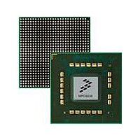
MPC8536DS Freescale Semiconductor, MPC8536DS Datasheet - Page 1688

MPC8536DS
Manufacturer Part Number
MPC8536DS
Description
BOARD DEV SYSTEM MPC8536E
Manufacturer
Freescale Semiconductor
Series
PowerQUICC III™r
Type
MPUr
Datasheets
1.MPC8536EBVTAVLA.pdf
(127 pages)
2.MPC8536EBVTAVLA.pdf
(1706 pages)
3.MPC8536DS.pdf
(2 pages)
4.MPC8536DS.pdf
(126 pages)
Specifications of MPC8536DS
Contents
Board, Software and Documentation
Processor Series
MPC85xx
Core
e500
Data Bus Width
32 bit
Maximum Clock Frequency
667 MHz
Operating Supply Voltage
- 0.3 V to + 1.21 V
Maximum Operating Temperature
+ 105 C
Data Ram Size
32 KB
Interface Type
SPI, USB
Program Memory Type
DDR2, DDR3, SDRAM
Core Size
32 Bit
Program Memory Size
544KB
Cpu Speed
1.5GHz
Digital Ic Case Style
BGA
No. Of Pins
783
Supply Voltage Range
0.95V To 1.05V
Rohs Compliant
Yes
For Use With/related Products
MPC8536
Lead Free Status / RoHS Status
Lead free / RoHS Compliant
- MPC8536EBVTAVLA PDF datasheet
- MPC8536EBVTAVLA PDF datasheet #2
- MPC8536DS PDF datasheet #3
- MPC8536DS PDF datasheet #4
- Current page: 1688 of 1706
- Download datasheet (15Mb)
D–D
Coherency rules
Commands
Communications processor module (CPM)
Configuration
Configuration space
Configuration, control, and status
Index-2
device clock signals summary, 4-3
device clocking operation, 4-24–4-27
eTSEC
I
LBC bus clocks and clock ratios, 13-4
PCI/PCI-X clocking, 16-45, 16-50
POR settings
L2 cache, 6-28
PCI, see PCI/PCI-X controller
serial peripheral interface (SPI)
DDR, 8-12–8-51, 8-62
ECM
eTSEC interfaces, 14-207–??
LBC
PCI/PCI-X
PIC
POR, see Power-on-reset (POR)
PCI Express, 17-43
PCI/PCI-X addressing, 16-48
accessing CCSR memory from external masters, 2-11
accessing CCSRs, 4-4
alternate configuration space (ALTBAR and ALTCAR),
boot page translation, 4-7
2
C
see also Signals, clock
CCB (platform) clock, 4-24
Ethernet clocks, 4-26
PCI Express clocks, 4-25
system clock/PCI clock, 4-24
inputs and outputs, 14-10
management clock out (EC_MDC), 14-11, 14-81
clock stretching, 11-17
clock synchronization, 11-16
input synchronization and digital filter, 11-16
clock ratio register (LCRR), 13-34
e500 core PLL ratio, 4-12
system/CCB PLL ratio, 4-11
multi-master operation, 18-3
CCB address configuration register (EEBACR), 7-3
CCB port configuration register (EEBPCR), 7-4
configuration register (LBCR), 13-32
configuration access registers, 16-60
configuration cycles, 16-58
configuration space header, 16-58
global configuration register, 9-21
minimum CCB frequency equations, 4-26
4-5
MPC8536E PowerQUICC III Integrated Processor Reference Manual, Rev. 1
Context ID registers, 25-22–25-23
Controller registers, 10-50
Crypto-channel
Crypto-channel registers, 10-37
CTS, see DUART_CTS[0:1]
D
Data cache
Data encryption standard execution units (DEU), 10-57,
DDR controller
CCSR memory map, 2-10–2-14
CCSRBAR update guidelines, 4-4
memory map/register definition, 4-3
organization of CCSR memory, 2-11
configuration register, 10-37
see L2 cache/SRAM
address signal mappings, 8-5
battery-backed RAM and forced self-refresh mode, 8-94
block diagram, 8-2, 8-60
clock distribution, 8-76
clocks
configuration, example, 8-62
data beat ordering, 8-83
debug mode
driver impedance calibration, 8-9
error checking and correcting (ECC), 6-39, 8-84
error handling, 8-53, 8-86
features, 8-2
functional description, 8-60
initialization/application information, 8-87
interrupts, 8-57
memory map/register definition, 8-10
modes of operation, 8-3
on-die termination for CSs, 8-9
page mode and logical bank retention, 8-83
performance monitor events, 24-17
register descriptions, 8-12
SDRAM operation, 8-64
10-108, 10-117
disabling, 23-32, 23-33
signal selection (POR), 4-23
source and target ID, 25-4, 25-24
testing ECC with error injection, 8-51–8-53
programming different memory types, 8-89
by acronym, see Register Index
configuration registers, 8-12–8-51
error handling registers, 8-53–8-60
error injection registers, 8-51–8-53
address multiplexing, 8-66
initialization sequence, 8-94
JEDEC standard interface commands, 8-71
mode-set command timing, 8-76
Freescale Semiconductor
Index
Related parts for MPC8536DS
Image
Part Number
Description
Manufacturer
Datasheet
Request
R
Part Number:
Description:
Manufacturer:
Freescale Semiconductor, Inc
Datasheet:
Part Number:
Description:
Manufacturer:
Freescale Semiconductor, Inc
Datasheet:
Part Number:
Description:
Manufacturer:
Freescale Semiconductor, Inc
Datasheet:
Part Number:
Description:
Manufacturer:
Freescale Semiconductor, Inc
Datasheet:
Part Number:
Description:
Manufacturer:
Freescale Semiconductor, Inc
Datasheet:
Part Number:
Description:
Manufacturer:
Freescale Semiconductor, Inc
Datasheet:
Part Number:
Description:
Manufacturer:
Freescale Semiconductor, Inc
Datasheet:
Part Number:
Description:
Manufacturer:
Freescale Semiconductor, Inc
Datasheet:
Part Number:
Description:
Manufacturer:
Freescale Semiconductor, Inc
Datasheet:
Part Number:
Description:
Manufacturer:
Freescale Semiconductor, Inc
Datasheet:
Part Number:
Description:
Manufacturer:
Freescale Semiconductor, Inc
Datasheet:
Part Number:
Description:
Manufacturer:
Freescale Semiconductor, Inc
Datasheet:
Part Number:
Description:
Manufacturer:
Freescale Semiconductor, Inc
Datasheet:
Part Number:
Description:
Manufacturer:
Freescale Semiconductor, Inc
Datasheet:
Part Number:
Description:
Manufacturer:
Freescale Semiconductor, Inc
Datasheet:


