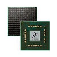
MPC8536DS Freescale Semiconductor, MPC8536DS Datasheet - Page 194

MPC8536DS
Manufacturer Part Number
MPC8536DS
Description
BOARD DEV SYSTEM MPC8536E
Manufacturer
Freescale Semiconductor
Series
PowerQUICC III™r
Type
MPUr
Datasheets
1.MPC8536EBVTAVLA.pdf
(127 pages)
2.MPC8536EBVTAVLA.pdf
(1706 pages)
3.MPC8536DS.pdf
(2 pages)
4.MPC8536DS.pdf
(126 pages)
Specifications of MPC8536DS
Contents
Board, Software and Documentation
Processor Series
MPC85xx
Core
e500
Data Bus Width
32 bit
Maximum Clock Frequency
667 MHz
Operating Supply Voltage
- 0.3 V to + 1.21 V
Maximum Operating Temperature
+ 105 C
Data Ram Size
32 KB
Interface Type
SPI, USB
Program Memory Type
DDR2, DDR3, SDRAM
Core Size
32 Bit
Program Memory Size
544KB
Cpu Speed
1.5GHz
Digital Ic Case Style
BGA
No. Of Pins
783
Supply Voltage Range
0.95V To 1.05V
Rohs Compliant
Yes
For Use With/related Products
MPC8536
Lead Free Status / RoHS Status
Lead free / RoHS Compliant
- MPC8536EBVTAVLA PDF datasheet
- MPC8536EBVTAVLA PDF datasheet #2
- MPC8536DS PDF datasheet #3
- MPC8536DS PDF datasheet #4
- Current page: 194 of 1706
- Download datasheet (15Mb)
Reset, Clocking, and Initialization
4.4.3.24
The LBC address/data bus inputs, shown in
configuration register defined in
(GPPORCR).”
LAD[0:31] during POR is captured and stored (read only) in the GPPORCR. Software can then use this
value to inform the operating system about initial system configuration. Typical interpretations include
circuit board type, board ID number, or a list of available peripherals.
4.4.3.25
These POR configuration inputs may be used in the future to control functionality. It is advised
that boards are built with the ability to pull up or pull down these pins. Note that the value latched
on these signals during POR are accessible through the PORDEVSR2, described in
Section 23.4.1.6, “POR Device Status Register 2
4.4.4
The following paragraphs describe the clocking within the device.
4.4.4.1
The MPC8536E takes a single input clock, SYSCLK, as its primary clock source for the e500 core and all
of the devices and interfaces that operate synchronously with the core. As shown in
SYSCLK input (frequency) is multiplied up using a phase lock loop (PLL) to create the core complex bus
(CCB) clock (also called the platform clock). The CCB clock is used by virtually all of the synchronous
system logic, including the L2 cache, and other internal blocks such as the DMA and interrupt controller.
The CCB clock also feeds the PLL in the e500 core and the PLL that create clocks for the local bus memory
controller.
The PCI interface may use SYSCLK as the PCI clock and thus have PCI operation be synchronous with the
platform. Alternately, a separate, independent clock may be used for the PCI interface, in which case PCI
4-24
TSEC1_TXD3,
TSEC3_TXD7
Functional
Default (111)
No default
LAD[0:31]
Functional
Signals
EC_MDC,
Signal
Clocking
General-Purpose POR Configuration
Engineering Use POR Configuration
System Clock/PCI Clock/DDR Clock
Reset Configuration
This register is intended to facilitate POR configuration of user systems. A value placed on
Reset Configuration
cfg_gpinput[0:31]
cfg_eng_use[0:2]
MPC8536E PowerQUICC III Integrated Processor Reference Manual, Rev. 1
Name
Name
Table 4-32. General-Purpose POR Configuration
Table 4-33. Engineering Use POR Configuration
Section 23.4.1.7, “General-Purpose POR Configuration Register
(Binary)
Value
(Binary)
000–110 Reserved
—
Value
111
General-purpose POR configuration vector to be placed in GPPORCR
Table
Default operation
4-32, configure the value of the general-purpose POR
(PORDEVSR2).”
Meaning
Meaning
Freescale Semiconductor
Figure
4-6, the
Related parts for MPC8536DS
Image
Part Number
Description
Manufacturer
Datasheet
Request
R
Part Number:
Description:
Manufacturer:
Freescale Semiconductor, Inc
Datasheet:
Part Number:
Description:
Manufacturer:
Freescale Semiconductor, Inc
Datasheet:
Part Number:
Description:
Manufacturer:
Freescale Semiconductor, Inc
Datasheet:
Part Number:
Description:
Manufacturer:
Freescale Semiconductor, Inc
Datasheet:
Part Number:
Description:
Manufacturer:
Freescale Semiconductor, Inc
Datasheet:
Part Number:
Description:
Manufacturer:
Freescale Semiconductor, Inc
Datasheet:
Part Number:
Description:
Manufacturer:
Freescale Semiconductor, Inc
Datasheet:
Part Number:
Description:
Manufacturer:
Freescale Semiconductor, Inc
Datasheet:
Part Number:
Description:
Manufacturer:
Freescale Semiconductor, Inc
Datasheet:
Part Number:
Description:
Manufacturer:
Freescale Semiconductor, Inc
Datasheet:
Part Number:
Description:
Manufacturer:
Freescale Semiconductor, Inc
Datasheet:
Part Number:
Description:
Manufacturer:
Freescale Semiconductor, Inc
Datasheet:
Part Number:
Description:
Manufacturer:
Freescale Semiconductor, Inc
Datasheet:
Part Number:
Description:
Manufacturer:
Freescale Semiconductor, Inc
Datasheet:
Part Number:
Description:
Manufacturer:
Freescale Semiconductor, Inc
Datasheet:


