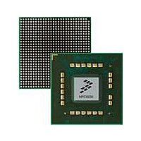
MPC8536DS Freescale Semiconductor, MPC8536DS Datasheet - Page 1308

MPC8536DS
Manufacturer Part Number
MPC8536DS
Description
BOARD DEV SYSTEM MPC8536E
Manufacturer
Freescale Semiconductor
Series
PowerQUICC III™r
Type
MPUr
Datasheets
1.MPC8536EBVTAVLA.pdf
(127 pages)
2.MPC8536EBVTAVLA.pdf
(1706 pages)
3.MPC8536DS.pdf
(2 pages)
4.MPC8536DS.pdf
(126 pages)
Specifications of MPC8536DS
Contents
Board, Software and Documentation
Processor Series
MPC85xx
Core
e500
Data Bus Width
32 bit
Maximum Clock Frequency
667 MHz
Operating Supply Voltage
- 0.3 V to + 1.21 V
Maximum Operating Temperature
+ 105 C
Data Ram Size
32 KB
Interface Type
SPI, USB
Program Memory Type
DDR2, DDR3, SDRAM
Core Size
32 Bit
Program Memory Size
544KB
Cpu Speed
1.5GHz
Digital Ic Case Style
BGA
No. Of Pins
783
Supply Voltage Range
0.95V To 1.05V
Rohs Compliant
Yes
For Use With/related Products
MPC8536
Lead Free Status / RoHS Status
Lead free / RoHS Compliant
- MPC8536EBVTAVLA PDF datasheet
- MPC8536EBVTAVLA PDF datasheet #2
- MPC8536DS PDF datasheet #3
- MPC8536DS PDF datasheet #4
- Current page: 1308 of 1706
- Download datasheet (15Mb)
Enhanced Secure Digital Host Controller
20.4.15 Watermark Level Register (WML)
Both write and read watermark levels are configurable. The value can be any number from 1–128 words.
20.4.16 Force Event Register (FEVT)
The force event register is not a physically implemented register. Rather, it is an address to which the
IRQSTAT register can be written if the corresponding bit of IRQSTATEN is set. Therefore, this register is
a write-only register and writing zero has no effect. Writing 1 to this register sets the corresponding bit of
IRQSTAT. Reading from this register always returns zeroes.
Forcing a card interrupt generates a short pulse on the SDHC_DAT[1] line, and the driver may treat this
interrupt as normal. The interrupt service routine may skip polling the card-interrupt source as the interrupt
is self-cleared.
20-34
Reset
Offset: 0x044 (WML)
WR_WML
13–15
16–31
RD_WML
Field
MBL
16–23
24–31
Field
8–15
W
0–7
R
0
0
0
Max block length. Indicates the maximum block size that the host driver can read and write to the buffer in the
eSDHC. The buffer should transfer block size without wait cycles.
000 512 bytes
001 1024 bytes
010 2048 bytes
011 4096 bytes
Reserved
0
Reserved
Write watermark level. Number of 32-bit words of watermark level in DMA write operation. Also, the number
of words of write burst length.
Note: The minimum value is 0x02, which represents 2 words (8 bytes).
Reserved
Read watermark level. Number of 32-bit words of watermark level in DMA read operation. Also, the number
of words of read burst length.
Note: The minimum value for RD_WML is 0x02, which means 2 words (8 bytes), and the maximum value
0
MPC8536E PowerQUICC III Integrated Processor Reference Manual, Rev. 1
—
0
for RD_WML is 0x10, which means 16 words (64 bytes). Setting RD_WML to values outside this
range results in non-predicted behavior.
Table 20-22. HOSTCAPBLT Field Descriptions (continued)
0
0
Figure 20-17. Watermark Level Register (WML)
0
7
0
8
Table 20-23. WML Field Descriptions
0
0
WR_WML
1
0
0
0
Description
15 16
0
Description
0
0
0
0
—
0
0
0
23 24
0
0
Freescale Semiconductor
0
0
Access: Read/Write
RD_WML
1
0
0
0
31
0
Related parts for MPC8536DS
Image
Part Number
Description
Manufacturer
Datasheet
Request
R
Part Number:
Description:
Manufacturer:
Freescale Semiconductor, Inc
Datasheet:
Part Number:
Description:
Manufacturer:
Freescale Semiconductor, Inc
Datasheet:
Part Number:
Description:
Manufacturer:
Freescale Semiconductor, Inc
Datasheet:
Part Number:
Description:
Manufacturer:
Freescale Semiconductor, Inc
Datasheet:
Part Number:
Description:
Manufacturer:
Freescale Semiconductor, Inc
Datasheet:
Part Number:
Description:
Manufacturer:
Freescale Semiconductor, Inc
Datasheet:
Part Number:
Description:
Manufacturer:
Freescale Semiconductor, Inc
Datasheet:
Part Number:
Description:
Manufacturer:
Freescale Semiconductor, Inc
Datasheet:
Part Number:
Description:
Manufacturer:
Freescale Semiconductor, Inc
Datasheet:
Part Number:
Description:
Manufacturer:
Freescale Semiconductor, Inc
Datasheet:
Part Number:
Description:
Manufacturer:
Freescale Semiconductor, Inc
Datasheet:
Part Number:
Description:
Manufacturer:
Freescale Semiconductor, Inc
Datasheet:
Part Number:
Description:
Manufacturer:
Freescale Semiconductor, Inc
Datasheet:
Part Number:
Description:
Manufacturer:
Freescale Semiconductor, Inc
Datasheet:
Part Number:
Description:
Manufacturer:
Freescale Semiconductor, Inc
Datasheet:


