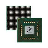
MPC8536DS Freescale Semiconductor, MPC8536DS Datasheet - Page 232

MPC8536DS
Manufacturer Part Number
MPC8536DS
Description
BOARD DEV SYSTEM MPC8536E
Manufacturer
Freescale Semiconductor
Series
PowerQUICC III™r
Type
MPUr
Datasheets
1.MPC8536EBVTAVLA.pdf
(127 pages)
2.MPC8536EBVTAVLA.pdf
(1706 pages)
3.MPC8536DS.pdf
(2 pages)
4.MPC8536DS.pdf
(126 pages)
Specifications of MPC8536DS
Contents
Board, Software and Documentation
Processor Series
MPC85xx
Core
e500
Data Bus Width
32 bit
Maximum Clock Frequency
667 MHz
Operating Supply Voltage
- 0.3 V to + 1.21 V
Maximum Operating Temperature
+ 105 C
Data Ram Size
32 KB
Interface Type
SPI, USB
Program Memory Type
DDR2, DDR3, SDRAM
Core Size
32 Bit
Program Memory Size
544KB
Cpu Speed
1.5GHz
Digital Ic Case Style
BGA
No. Of Pins
783
Supply Voltage Range
0.95V To 1.05V
Rohs Compliant
Yes
For Use With/related Products
MPC8536
Lead Free Status / RoHS Status
Lead free / RoHS Compliant
- MPC8536EBVTAVLA PDF datasheet
- MPC8536EBVTAVLA PDF datasheet #2
- MPC8536DS PDF datasheet #3
- MPC8536DS PDF datasheet #4
- Current page: 232 of 1706
- Download datasheet (15Mb)
L2 Look-Aside Cache/SRAM
6-12
22–23
24–27
Bits
18
19
20
21
28
L2STASHDIS
L2LFRID
L2SLC
L2LFR
Name
L2LO
—
—
MPC8536E PowerQUICC III Integrated Processor Reference Manual, Rev. 1
L2 cache lock overflow. Reserved in full memory-mapped SRAM mode. This sticky bit is set if an
overlock condition is detected in the L2 cache. A lock overflow is triggered either by executing
instruction or data cache block touch and lock set instructions or by performing L2 cache external
writes with lock set. If all ways are locked and an attempt to stash is made, the stash is not allocated.
0 The L2 cache did not encounter a lock overflow. L2LO is cleared only by software.
1 The L2 cache encountered a lock overflow condition.
L2 snoop lock clear. This sticky bit is set if a snoop invalidated a locked data cache line. Note that the
lock bit for that line is cleared whenever the line is invalidated. L2SLC is reserved in full
memory-mapped SRAM mode.
0 A snoop did not invalidate a locked L2 cache line. L2SLC is cleared only by software.
1 The L2 cache encountered a snoop that invalidated a locked line.
Reserved
L2 cache lock bits flash reset. The L2 cache must be enabled (L2CTL[L2E] = 1) for reset to occur. This
field is reserved in full memory-mapped SRAM mode.
0 The L2 cache lock bits are not cleared or the clear operation completed.
1 A reset operation is issued that clears each L2 cache line’s lock bits. Depending on the L2LFRID
L2 cache lock bits flash reset select instruction or data. Indicates whether data or instruction lock bits
or both are reset.
00 Not used
01 Reset data locks if L2LFR = 1.
10 Reset instruction locks if L2LFR = 1.
11 Reset both data and instruction locks if L2LFR = 1.
Reserved
L2 stash allocate disable. Disables allocation of lines for stashing.
0 The L2 cache allocate lines for global writes that hit in a stash range or that have the stashing
1 The L2 does not allocate lines for stashed writes.
Note: This bit does NOT affect the updating of lines that are already resident in the cache and have
value, data or instruction locks, or both, can be reset. Cache access is blocked during this time. After
L2LFR is set, the L2 cache unit automatically clears L2LFR when the reset operation is complete
(if L2CTL[L2E] is set).
attribute set.
the stash attribute set or hit a stash range. Such lines are updated even if this bit is set.To
change this bit, the L2 must be disabled (L2CTL[L2E] = 0).
Table 6-4. L2CTL Field Descriptions (continued)
Description
Freescale Semiconductor
Related parts for MPC8536DS
Image
Part Number
Description
Manufacturer
Datasheet
Request
R
Part Number:
Description:
Manufacturer:
Freescale Semiconductor, Inc
Datasheet:
Part Number:
Description:
Manufacturer:
Freescale Semiconductor, Inc
Datasheet:
Part Number:
Description:
Manufacturer:
Freescale Semiconductor, Inc
Datasheet:
Part Number:
Description:
Manufacturer:
Freescale Semiconductor, Inc
Datasheet:
Part Number:
Description:
Manufacturer:
Freescale Semiconductor, Inc
Datasheet:
Part Number:
Description:
Manufacturer:
Freescale Semiconductor, Inc
Datasheet:
Part Number:
Description:
Manufacturer:
Freescale Semiconductor, Inc
Datasheet:
Part Number:
Description:
Manufacturer:
Freescale Semiconductor, Inc
Datasheet:
Part Number:
Description:
Manufacturer:
Freescale Semiconductor, Inc
Datasheet:
Part Number:
Description:
Manufacturer:
Freescale Semiconductor, Inc
Datasheet:
Part Number:
Description:
Manufacturer:
Freescale Semiconductor, Inc
Datasheet:
Part Number:
Description:
Manufacturer:
Freescale Semiconductor, Inc
Datasheet:
Part Number:
Description:
Manufacturer:
Freescale Semiconductor, Inc
Datasheet:
Part Number:
Description:
Manufacturer:
Freescale Semiconductor, Inc
Datasheet:
Part Number:
Description:
Manufacturer:
Freescale Semiconductor, Inc
Datasheet:


