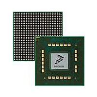
MPC8536DS Freescale Semiconductor, MPC8536DS Datasheet - Page 726

MPC8536DS
Manufacturer Part Number
MPC8536DS
Description
BOARD DEV SYSTEM MPC8536E
Manufacturer
Freescale Semiconductor
Series
PowerQUICC III™r
Type
MPUr
Datasheets
1.MPC8536EBVTAVLA.pdf
(127 pages)
2.MPC8536EBVTAVLA.pdf
(1706 pages)
3.MPC8536DS.pdf
(2 pages)
4.MPC8536DS.pdf
(126 pages)
Specifications of MPC8536DS
Contents
Board, Software and Documentation
Processor Series
MPC85xx
Core
e500
Data Bus Width
32 bit
Maximum Clock Frequency
667 MHz
Operating Supply Voltage
- 0.3 V to + 1.21 V
Maximum Operating Temperature
+ 105 C
Data Ram Size
32 KB
Interface Type
SPI, USB
Program Memory Type
DDR2, DDR3, SDRAM
Core Size
32 Bit
Program Memory Size
544KB
Cpu Speed
1.5GHz
Digital Ic Case Style
BGA
No. Of Pins
783
Supply Voltage Range
0.95V To 1.05V
Rohs Compliant
Yes
For Use With/related Products
MPC8536
Lead Free Status / RoHS Status
Lead free / RoHS Compliant
- MPC8536EBVTAVLA PDF datasheet
- MPC8536EBVTAVLA PDF datasheet #2
- MPC8536DS PDF datasheet #3
- MPC8536DS PDF datasheet #4
- Current page: 726 of 1706
- Download datasheet (15Mb)
Enhanced Local Bus Controller
13.4.4.4.2
If BRn[MSEL] of the accessed bank selects a UPM on the currently requested cycle, the UPM manipulates
the LCSn for that bank with timing as specified in the UPM RAM word CSTn fields. The selected UPM
affects only the assertion and negation of the appropriate LCSn signal. The state of the selected LCSn
signal of the corresponding bank depends on the value of each CSTn bit.
control LCSn signals.
13.4.4.4.3
If BRn[MSEL] of the accessed memory bank selects a UPM on the currently requested cycle, the selected
UPM affects the assertion and negation of the appropriate LBS[0:3] signal. The timing of all four
byte-select signals is specified in the RAM word. However, LBS[0:3] are also controlled by the port size
of the accessed bank, the number of bytes to transfer, and the address accessed.
UPMs control LBS[0:3].
13-84
Bits
31
Name
LAST
Chip-Select Signal Timing (CST n )
Byte Select Signal Timing (BST n )
UPMA/B/C
MPC8536E PowerQUICC III Integrated Processor Reference Manual, Rev. 1
GPCM
FCM
signal timing set in the RAM word is applied to the current (and last) cycle. However, if the
disable timer is activated and the next access is to the same bank, execution of the next UPM
pattern is held off and the control signal values specified in the last word are extended in
duration for the number of clock cycles specified in M x MR[DS n ].
0 The UPM continues executing RAM words.
1 Indicates the last RAM word in the program. The service to the UPM request is done after
In case of UPM writes, program UTA and LAST in same RAM word.
In case of UPM reads, program UTA and LAST in consecutive or same RAM words.
Last word. When LAST is read in a RAM word, the current UPM pattern terminates and control
this cycle concludes.
Table 13-40. RAM Word Field Descriptions (continued)
Figure 13-67. LCS n Signal Selection
Bank Selected
BR n [MSEL]
MUX
Description
Switch
Figure 13-67
Figure 13-68
Freescale Semiconductor
LCS0
LCS1
LCS2
LCS3
LCS4
LCS5
LCS6
LCS7
shows how UPMs
shows how
Related parts for MPC8536DS
Image
Part Number
Description
Manufacturer
Datasheet
Request
R
Part Number:
Description:
Manufacturer:
Freescale Semiconductor, Inc
Datasheet:
Part Number:
Description:
Manufacturer:
Freescale Semiconductor, Inc
Datasheet:
Part Number:
Description:
Manufacturer:
Freescale Semiconductor, Inc
Datasheet:
Part Number:
Description:
Manufacturer:
Freescale Semiconductor, Inc
Datasheet:
Part Number:
Description:
Manufacturer:
Freescale Semiconductor, Inc
Datasheet:
Part Number:
Description:
Manufacturer:
Freescale Semiconductor, Inc
Datasheet:
Part Number:
Description:
Manufacturer:
Freescale Semiconductor, Inc
Datasheet:
Part Number:
Description:
Manufacturer:
Freescale Semiconductor, Inc
Datasheet:
Part Number:
Description:
Manufacturer:
Freescale Semiconductor, Inc
Datasheet:
Part Number:
Description:
Manufacturer:
Freescale Semiconductor, Inc
Datasheet:
Part Number:
Description:
Manufacturer:
Freescale Semiconductor, Inc
Datasheet:
Part Number:
Description:
Manufacturer:
Freescale Semiconductor, Inc
Datasheet:
Part Number:
Description:
Manufacturer:
Freescale Semiconductor, Inc
Datasheet:
Part Number:
Description:
Manufacturer:
Freescale Semiconductor, Inc
Datasheet:
Part Number:
Description:
Manufacturer:
Freescale Semiconductor, Inc
Datasheet:


