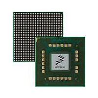
MPC8536DS Freescale Semiconductor, MPC8536DS Datasheet - Page 666

MPC8536DS
Manufacturer Part Number
MPC8536DS
Description
BOARD DEV SYSTEM MPC8536E
Manufacturer
Freescale Semiconductor
Series
PowerQUICC III™r
Type
MPUr
Datasheets
1.MPC8536EBVTAVLA.pdf
(127 pages)
2.MPC8536EBVTAVLA.pdf
(1706 pages)
3.MPC8536DS.pdf
(2 pages)
4.MPC8536DS.pdf
(126 pages)
Specifications of MPC8536DS
Contents
Board, Software and Documentation
Processor Series
MPC85xx
Core
e500
Data Bus Width
32 bit
Maximum Clock Frequency
667 MHz
Operating Supply Voltage
- 0.3 V to + 1.21 V
Maximum Operating Temperature
+ 105 C
Data Ram Size
32 KB
Interface Type
SPI, USB
Program Memory Type
DDR2, DDR3, SDRAM
Core Size
32 Bit
Program Memory Size
544KB
Cpu Speed
1.5GHz
Digital Ic Case Style
BGA
No. Of Pins
783
Supply Voltage Range
0.95V To 1.05V
Rohs Compliant
Yes
For Use With/related Products
MPC8536
Lead Free Status / RoHS Status
Lead free / RoHS Compliant
- MPC8536EBVTAVLA PDF datasheet
- MPC8536EBVTAVLA PDF datasheet #2
- MPC8536DS PDF datasheet #3
- MPC8536DS PDF datasheet #4
- Current page: 666 of 1706
- Download datasheet (15Mb)
Enhanced Local Bus Controller
must be set up before issuing a write command to the UPM, or before issuing a FCM operation sequence
that uses MDR to source address or data bytes.
Table 13-13
13.3.1.7
The special operation initiation register (LSOR), shown in
special operation on the indicated bank. Writing to LSOR activates a special operation on bank
LSOR[BANK] provided that the bank is valid and controlled by a memory controller whose mode OP field
is set to a value other than ‘normal operation.’ If eLBC is currently busy with a memory transaction,
writing LSOR completes immediately, but the special operation request is queued until eLBC can service
it. To avoid race conditions between software and a busy eLBC, registers that affect currently running
special operation and LSOR must not be re-written before a pending special operation has been completed.
The UPM and FCM have different indications of when such special operations are completed. The
behavior of eLBC is unpredictable if special operation modes are altered between LSOR being written and
the relevant memory controller completing that access.
13-24
16–23
24–31
Offset 0x0_5088
Offset 0x0_5088
Reset
Reset
0–31
8–15
Bits
0–7
W
W
R
R
0
0
Name
AS3
AS2
AS1
AS0
D
describes MDR[D].
Special Operation Initiation Register (LSOR)
In UPM mode, D is the data to be read or written into the RAM array when a write or read command is
supplied to the UPM (M x MR[OP] = 01 or M x MR[OP] = 10).
In FCM mode, AS3 is the fourth byte of address sent by a custom address write operation, or the fourth byte
of data read from a read status operation.
In FCM mode, AS2 is the third byte of address sent by a custom address write operation, or the third byte of
data read from a read status operation.
In FCM mode, AS1 is the second byte of address sent by a custom address write operation, or the second
byte of data read from a read status operation.
In FCM mode, AS0 is the first byte of address sent by a custom address write operation, or the first byte of
data read from a read status operation.
AS3
MPC8536E PowerQUICC III Integrated Processor Reference Manual, Rev. 1
Figure 13-10. FCM Data Register in FCM Mode (MDR)
Figure 13-9. UPM Data Register in UPM Mode (MDR)
7
8
Table 13-13. MDR Field Description
AS2
All zeros
All zeros
15 16
Description
D
Figure
13-11, is used by software to trigger a
AS1
23 24
Freescale Semiconductor
Access: Read/Write
Access: Read/Write
AS0
31
31
Related parts for MPC8536DS
Image
Part Number
Description
Manufacturer
Datasheet
Request
R
Part Number:
Description:
Manufacturer:
Freescale Semiconductor, Inc
Datasheet:
Part Number:
Description:
Manufacturer:
Freescale Semiconductor, Inc
Datasheet:
Part Number:
Description:
Manufacturer:
Freescale Semiconductor, Inc
Datasheet:
Part Number:
Description:
Manufacturer:
Freescale Semiconductor, Inc
Datasheet:
Part Number:
Description:
Manufacturer:
Freescale Semiconductor, Inc
Datasheet:
Part Number:
Description:
Manufacturer:
Freescale Semiconductor, Inc
Datasheet:
Part Number:
Description:
Manufacturer:
Freescale Semiconductor, Inc
Datasheet:
Part Number:
Description:
Manufacturer:
Freescale Semiconductor, Inc
Datasheet:
Part Number:
Description:
Manufacturer:
Freescale Semiconductor, Inc
Datasheet:
Part Number:
Description:
Manufacturer:
Freescale Semiconductor, Inc
Datasheet:
Part Number:
Description:
Manufacturer:
Freescale Semiconductor, Inc
Datasheet:
Part Number:
Description:
Manufacturer:
Freescale Semiconductor, Inc
Datasheet:
Part Number:
Description:
Manufacturer:
Freescale Semiconductor, Inc
Datasheet:
Part Number:
Description:
Manufacturer:
Freescale Semiconductor, Inc
Datasheet:
Part Number:
Description:
Manufacturer:
Freescale Semiconductor, Inc
Datasheet:


