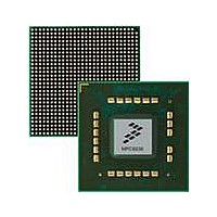
MPC8536DS Freescale Semiconductor, MPC8536DS Datasheet - Page 1285

MPC8536DS
Manufacturer Part Number
MPC8536DS
Description
BOARD DEV SYSTEM MPC8536E
Manufacturer
Freescale Semiconductor
Series
PowerQUICC III™r
Type
MPUr
Datasheets
1.MPC8536EBVTAVLA.pdf
(127 pages)
2.MPC8536EBVTAVLA.pdf
(1706 pages)
3.MPC8536DS.pdf
(2 pages)
4.MPC8536DS.pdf
(126 pages)
Specifications of MPC8536DS
Contents
Board, Software and Documentation
Processor Series
MPC85xx
Core
e500
Data Bus Width
32 bit
Maximum Clock Frequency
667 MHz
Operating Supply Voltage
- 0.3 V to + 1.21 V
Maximum Operating Temperature
+ 105 C
Data Ram Size
32 KB
Interface Type
SPI, USB
Program Memory Type
DDR2, DDR3, SDRAM
Core Size
32 Bit
Program Memory Size
544KB
Cpu Speed
1.5GHz
Digital Ic Case Style
BGA
No. Of Pins
783
Supply Voltage Range
0.95V To 1.05V
Rohs Compliant
Yes
For Use With/related Products
MPC8536
Lead Free Status / RoHS Status
Lead free / RoHS Compliant
- MPC8536EBVTAVLA PDF datasheet
- MPC8536EBVTAVLA PDF datasheet #2
- MPC8536DS PDF datasheet #3
- MPC8536DS PDF datasheet #4
- Current page: 1285 of 1706
- Download datasheet (15Mb)
20.4.5
The command response registers stores the four parts of the response bits from the card.
Table 20-9
registers for each response type. In the table, R[ ] refers to a bit range within the response data as
transmitted on the SD bus.
This table shows that:
To be able to read the response status efficiently, the eSDHC only stores part of the response data in the
command response registers. This enables the host driver to efficiently read 32 bits of response data in one
read cycle on a 32-bit bus system. Parts of the response, the index field, and the CRC are checked by the
eSDHC (as specified by XFERTYP[CICEN, CCCEN]) and generate an error interrupt if any error is
detected. The bit range for the CRC check depends on the response length. If the response length is 48, the
eSDHC checks R[47:1], and if the response length is 136, the eSDHC checks R[119:1].
Freescale Semiconductor
Reset
Offset: 0x010 (CMDRSP0)
•
•
•
W
R
Most responses with a length of 48 (R[47:0]) have 32 bits of the response data (R[39:8]) stored in
the CMDRSP0 register.
Responses of type R1b (Auto CMD12 responses) have response data bits R[39:8] stored in the
CMDRSP3 register.
Responses with length 136 (R[135:0]) have 120 bits of the response data (R[127:8]) stored in the
CMDRSP0, 1, 2, and 3 registers.
R1b (Auto CMD12 response)
0x014 (CMDRSP1)
0x018 (CMDRSP2)
0x01C (CMDRSP3)
R1,R1b (normal response)
0
R2 (CID, CSD register)
describes the mapping of command responses from the SD bus to the command response
Command Response 0–3 (CMDRSP0–3)
R3 (OCR register)
R4 (OCR register)
R6 (publish RCA)
Response Type
MPC8536E PowerQUICC III Integrated Processor Reference Manual, Rev. 1
Table 20-9. Response Bit Definition for Each Response Type
Figure 20-7. Command Response 0–3 Register (CMDRSP n )
Card status for Auto CMD12
New published RCA[31:16]
OCR register for memory
CID/CSD register [127:8]
OCR register for I/O etc.
Meaning of Response
and card status[15:0]
Card status
CMDRSP
All zeros
Response
R[127:8]
R[39:8]
R[39:8]
R[39:8]
R[39:8]
R[39:8]
Field
{CMDRSP3[23:0], CMDRSP2,
Enhanced Secure Digital Host Controller
CMDRSP1, CMDRSP0}
Response Register
CMDRSP0
CMDRSP3
CMDRSP0
CMDRSP0
CMDRSP0
Access: Read
20-11
31
Related parts for MPC8536DS
Image
Part Number
Description
Manufacturer
Datasheet
Request
R
Part Number:
Description:
Manufacturer:
Freescale Semiconductor, Inc
Datasheet:
Part Number:
Description:
Manufacturer:
Freescale Semiconductor, Inc
Datasheet:
Part Number:
Description:
Manufacturer:
Freescale Semiconductor, Inc
Datasheet:
Part Number:
Description:
Manufacturer:
Freescale Semiconductor, Inc
Datasheet:
Part Number:
Description:
Manufacturer:
Freescale Semiconductor, Inc
Datasheet:
Part Number:
Description:
Manufacturer:
Freescale Semiconductor, Inc
Datasheet:
Part Number:
Description:
Manufacturer:
Freescale Semiconductor, Inc
Datasheet:
Part Number:
Description:
Manufacturer:
Freescale Semiconductor, Inc
Datasheet:
Part Number:
Description:
Manufacturer:
Freescale Semiconductor, Inc
Datasheet:
Part Number:
Description:
Manufacturer:
Freescale Semiconductor, Inc
Datasheet:
Part Number:
Description:
Manufacturer:
Freescale Semiconductor, Inc
Datasheet:
Part Number:
Description:
Manufacturer:
Freescale Semiconductor, Inc
Datasheet:
Part Number:
Description:
Manufacturer:
Freescale Semiconductor, Inc
Datasheet:
Part Number:
Description:
Manufacturer:
Freescale Semiconductor, Inc
Datasheet:
Part Number:
Description:
Manufacturer:
Freescale Semiconductor, Inc
Datasheet:


