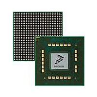
MPC8536DS Freescale Semiconductor, MPC8536DS Datasheet - Page 338

MPC8536DS
Manufacturer Part Number
MPC8536DS
Description
BOARD DEV SYSTEM MPC8536E
Manufacturer
Freescale Semiconductor
Series
PowerQUICC III™r
Type
MPUr
Datasheets
1.MPC8536EBVTAVLA.pdf
(127 pages)
2.MPC8536EBVTAVLA.pdf
(1706 pages)
3.MPC8536DS.pdf
(2 pages)
4.MPC8536DS.pdf
(126 pages)
Specifications of MPC8536DS
Contents
Board, Software and Documentation
Processor Series
MPC85xx
Core
e500
Data Bus Width
32 bit
Maximum Clock Frequency
667 MHz
Operating Supply Voltage
- 0.3 V to + 1.21 V
Maximum Operating Temperature
+ 105 C
Data Ram Size
32 KB
Interface Type
SPI, USB
Program Memory Type
DDR2, DDR3, SDRAM
Core Size
32 Bit
Program Memory Size
544KB
Cpu Speed
1.5GHz
Digital Ic Case Style
BGA
No. Of Pins
783
Supply Voltage Range
0.95V To 1.05V
Rohs Compliant
Yes
For Use With/related Products
MPC8536
Lead Free Status / RoHS Status
Lead free / RoHS Compliant
- MPC8536EBVTAVLA PDF datasheet
- MPC8536EBVTAVLA PDF datasheet #2
- MPC8536DS PDF datasheet #3
- MPC8536DS PDF datasheet #4
- Current page: 338 of 1706
- Download datasheet (15Mb)
DDR Memory Controller
8.5.1
The DDR memory controller supports many different DDR SDRAM configurations. SDRAMs with
different sizes can be used in the same system. Sixteen multiplexed address signals and three logical bank
select signals support device densities from 64 Mbits to 4 Gbits. Four chip select (CS) signals support up
to two DIMMs of memory. The DDR SDRAM physical banks can be built from standard memory modules
or directly-attached memory devices. The data path to individual physical banks is 64 or 32 bits wide, 72
or 40 bits with ECC. The DDR memory controller supports physical bank sizes from 16 Mbytes to
4 Gbytes. The physical banks can be constructed using x8, x16, or x32 memory devices. The memory
technologies supported are 64 Mbits, 128 Mbits, 256 Mbits, 512 Mbits, 1 Gbit, 2 Gbits, and 4 Gbits. Nine
data qualifier (DQM) signals provide byte selection for memory accesses.
When ECC is enabled, all memory accesses are performed on double-word boundaries (that is, all DQM
signals are set simultaneously). However, when ECC is disabled, the memory system uses the DQM
signals for byte lane selection.
Table 8-50
MDQS[0:7], and MDQ[0:63] when DDR SDRAM memories are used with x8 or x16 devices.
8.5.1.1
Although the DDR memory controller multiplexes row and column address bits onto 16 memory address
signals and 3 logical bank select signals, a physical bank may be implemented with memory devices
requiring fewer than 31 address bits. The physical bank may be configured to provide from 12 to 16 row
address bits, plus 2 or 3 logical bank-select bits and from 8–11 column address bits.
8-64
shows the DDR memory controller’s relationships between data byte lane0–7, MDM[0:7],
DDR SDRAM Interface Operation
Supported DDR SDRAM Organizations
An 8-bit DDR SDRAM device has a DQM signal and eight data signals
(DQ[0:7]). A 16-bit DDR SDRAM device has two DQM signals associated
with specific halves of the 16 data signals (DQ[0:7] and DQ[8:15]).
Data Byte Lane
MPC8536E PowerQUICC III Integrated Processor Reference Manual, Rev. 1
0 (MSB)
7 (LSB)
1
2
3
4
5
6
Table 8-50. Byte Lane to Data Relationship
Data Bus Mask
MDM[0]
MDM[1]
MDM[2]
MDM[3]
MDM[4]
MDM[5]
MDM[6]
MDM[7]
NOTE
Data Bus Strobe Data Bus 64-Bit Mode
MDQS[0]
MDQS[1]
MDQS[2]
MDQS[3]
MDQS[4]
MDQS[5]
MDQS[6]
MDQS[7]
MDQ[16:23]
MDQ[24:31]
MDQ[32:39]
MDQ[40:47]
MDQ[48:55]
MDQ[56:63]
MDQ[8:15]
MDQ[0:7]
Freescale Semiconductor
Related parts for MPC8536DS
Image
Part Number
Description
Manufacturer
Datasheet
Request
R
Part Number:
Description:
Manufacturer:
Freescale Semiconductor, Inc
Datasheet:
Part Number:
Description:
Manufacturer:
Freescale Semiconductor, Inc
Datasheet:
Part Number:
Description:
Manufacturer:
Freescale Semiconductor, Inc
Datasheet:
Part Number:
Description:
Manufacturer:
Freescale Semiconductor, Inc
Datasheet:
Part Number:
Description:
Manufacturer:
Freescale Semiconductor, Inc
Datasheet:
Part Number:
Description:
Manufacturer:
Freescale Semiconductor, Inc
Datasheet:
Part Number:
Description:
Manufacturer:
Freescale Semiconductor, Inc
Datasheet:
Part Number:
Description:
Manufacturer:
Freescale Semiconductor, Inc
Datasheet:
Part Number:
Description:
Manufacturer:
Freescale Semiconductor, Inc
Datasheet:
Part Number:
Description:
Manufacturer:
Freescale Semiconductor, Inc
Datasheet:
Part Number:
Description:
Manufacturer:
Freescale Semiconductor, Inc
Datasheet:
Part Number:
Description:
Manufacturer:
Freescale Semiconductor, Inc
Datasheet:
Part Number:
Description:
Manufacturer:
Freescale Semiconductor, Inc
Datasheet:
Part Number:
Description:
Manufacturer:
Freescale Semiconductor, Inc
Datasheet:
Part Number:
Description:
Manufacturer:
Freescale Semiconductor, Inc
Datasheet:


