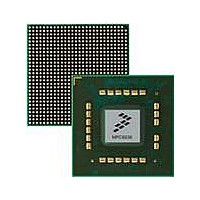
MPC8536DS Freescale Semiconductor, MPC8536DS Datasheet - Page 667

MPC8536DS
Manufacturer Part Number
MPC8536DS
Description
BOARD DEV SYSTEM MPC8536E
Manufacturer
Freescale Semiconductor
Series
PowerQUICC III™r
Type
MPUr
Datasheets
1.MPC8536EBVTAVLA.pdf
(127 pages)
2.MPC8536EBVTAVLA.pdf
(1706 pages)
3.MPC8536DS.pdf
(2 pages)
4.MPC8536DS.pdf
(126 pages)
Specifications of MPC8536DS
Contents
Board, Software and Documentation
Processor Series
MPC85xx
Core
e500
Data Bus Width
32 bit
Maximum Clock Frequency
667 MHz
Operating Supply Voltage
- 0.3 V to + 1.21 V
Maximum Operating Temperature
+ 105 C
Data Ram Size
32 KB
Interface Type
SPI, USB
Program Memory Type
DDR2, DDR3, SDRAM
Core Size
32 Bit
Program Memory Size
544KB
Cpu Speed
1.5GHz
Digital Ic Case Style
BGA
No. Of Pins
783
Supply Voltage Range
0.95V To 1.05V
Rohs Compliant
Yes
For Use With/related Products
MPC8536
Lead Free Status / RoHS Status
Lead free / RoHS Compliant
- MPC8536EBVTAVLA PDF datasheet
- MPC8536EBVTAVLA PDF datasheet #2
- MPC8536DS PDF datasheet #3
- MPC8536DS PDF datasheet #4
- Current page: 667 of 1706
- Download datasheet (15Mb)
UPM special operation modes are set in registers MxMR[OP], see
Registers (MxMR).”
Mode Register (FMR).”
performing a dummy access to a bank associated with the controller in question, but use of LSOR avoids
changing settings for the address space occupied by the bank. More details of special operation sequences
appear in
Table 13-14
13.3.1.8
The UPM refresh timer (LURT), shown in
selected a UPM machine and are refresh-enabled (MxMR[RFEN] = 1). Each time the timer expires, a
qualified bank generates a refresh request using the selected UPM. The qualified banks rotate their
requests.
Freescale Semiconductor
29–31
Offset 0x0_5090
Offset 0x0_50A0
Reset
0–28
Reset
Bits
W
W
R
R
0
0
Name
BANK Bank on which a special operation is initiated. If the bank identified by BANK is marked valid (BR n [V] set) and
Section 13.4.4.2.1, “UPM Programming Example (Two Sequential Writes to the RAM Array).”
—
describes LSOR.
UPM Refresh Timer (LURT)
Reserved
the bank is controlled by a memory controller whose current mode OP is non-zero—or a special
operation—eLBC will request the special operation to be activated on the selected bank when this field is
written. Otherwise, writing this field has no effect.
000 Bank 0 is triggered for special operation
...
111
LURT
MPC8536E PowerQUICC III Integrated Processor Reference Manual, Rev. 1
Bank 7 is triggered for special operation
FCM special operation modes are set in FMR[OP], see
Figure 13-11. Special Operation Initiation Register (LSOR)
Writing LSOR has the same effect as setting a special controller mode and
7
8
Figure 13-12. UPM Refresh Timer (LURT)
Table 13-14. LSOR Field Description
Figure
13-12, generates a refresh request for all valid banks that
—
All zeros
All zeros
Description
Section 13.3.1.4, “UPM Mode
—
Section 13.3.1.17, “Flash
Enhanced Local Bus Controller
Access: Read/Write
Access: Read/Write
28 29
BANK
13-25
31
31
Related parts for MPC8536DS
Image
Part Number
Description
Manufacturer
Datasheet
Request
R
Part Number:
Description:
Manufacturer:
Freescale Semiconductor, Inc
Datasheet:
Part Number:
Description:
Manufacturer:
Freescale Semiconductor, Inc
Datasheet:
Part Number:
Description:
Manufacturer:
Freescale Semiconductor, Inc
Datasheet:
Part Number:
Description:
Manufacturer:
Freescale Semiconductor, Inc
Datasheet:
Part Number:
Description:
Manufacturer:
Freescale Semiconductor, Inc
Datasheet:
Part Number:
Description:
Manufacturer:
Freescale Semiconductor, Inc
Datasheet:
Part Number:
Description:
Manufacturer:
Freescale Semiconductor, Inc
Datasheet:
Part Number:
Description:
Manufacturer:
Freescale Semiconductor, Inc
Datasheet:
Part Number:
Description:
Manufacturer:
Freescale Semiconductor, Inc
Datasheet:
Part Number:
Description:
Manufacturer:
Freescale Semiconductor, Inc
Datasheet:
Part Number:
Description:
Manufacturer:
Freescale Semiconductor, Inc
Datasheet:
Part Number:
Description:
Manufacturer:
Freescale Semiconductor, Inc
Datasheet:
Part Number:
Description:
Manufacturer:
Freescale Semiconductor, Inc
Datasheet:
Part Number:
Description:
Manufacturer:
Freescale Semiconductor, Inc
Datasheet:
Part Number:
Description:
Manufacturer:
Freescale Semiconductor, Inc
Datasheet:


