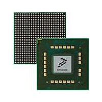
MPC8536DS Freescale Semiconductor, MPC8536DS Datasheet - Page 708

MPC8536DS
Manufacturer Part Number
MPC8536DS
Description
BOARD DEV SYSTEM MPC8536E
Manufacturer
Freescale Semiconductor
Series
PowerQUICC III™r
Type
MPUr
Datasheets
1.MPC8536EBVTAVLA.pdf
(127 pages)
2.MPC8536EBVTAVLA.pdf
(1706 pages)
3.MPC8536DS.pdf
(2 pages)
4.MPC8536DS.pdf
(126 pages)
Specifications of MPC8536DS
Contents
Board, Software and Documentation
Processor Series
MPC85xx
Core
e500
Data Bus Width
32 bit
Maximum Clock Frequency
667 MHz
Operating Supply Voltage
- 0.3 V to + 1.21 V
Maximum Operating Temperature
+ 105 C
Data Ram Size
32 KB
Interface Type
SPI, USB
Program Memory Type
DDR2, DDR3, SDRAM
Core Size
32 Bit
Program Memory Size
544KB
Cpu Speed
1.5GHz
Digital Ic Case Style
BGA
No. Of Pins
783
Supply Voltage Range
0.95V To 1.05V
Rohs Compliant
Yes
For Use With/related Products
MPC8536
Lead Free Status / RoHS Status
Lead free / RoHS Compliant
- MPC8536EBVTAVLA PDF datasheet
- MPC8536EBVTAVLA PDF datasheet #2
- MPC8536DS PDF datasheet #3
- MPC8536DS PDF datasheet #4
- Current page: 708 of 1706
- Download datasheet (15Mb)
Enhanced Local Bus Controller
13.4.3.2.1
There are two kinds of command instruction:
The manufacturer’s datasheet should be consulted to determine values for programming into the FCR
register, and whether a given command in the sequence is expected to initiate busy device behavior.
13.4.3.2.2
A NOP instruction that appears in FIR ahead of the last instruction is executed with the timing of a regular
command instruction, but neither LFCLE nor LFWE are asserted. Thus a NOP instruction may be used to
insert a pause matching the time taken for a regular command write.
13.4.3.2.3
Address instructions are used to issue addresses to the NAND Flash EEPROM. A complete device address
is formed from a sequence of one or more bytes, each written onto LAD[0:7] with LFALE and LFWE
asserted together. There are three kinds of address generation provided:
13-66
•
•
•
•
Commands that issue immediately—CM0, CM1, CM2, and CM3. These commands write a single
command byte by asserting LFCLE and LFWE while driving an 8-bit command onto LAD[0:7].
Op-code CMn sources its command byte from field FCR[CMDn], therefore up to four different
commands can be issued in any FCM instruction sequence.
Commands that wait for LFRB to be sampled high (EEPROM in ready state) before
issuing—CW0, and CW1. These commands first poll the LFRB pin, waiting for it to go high,
before writing a single command byte onto LAD[0:7], sourced from FCR[CMDn] for op-code
CWn. It is necessary to use CWn op-codes whenever the EEPROM is expected to be in a busy state
(such as following a page read, block erase, or program operation) and therefore initially
unresponsive to commands. To avoid deadlock in cases where the device is already available, FCM
does not expect a transition on LFRB. Rather, FCM waits for 8×(2+ORn[SCY]) clock cycles
(when ORn[TRLX] = 0) or 16×(2+ORn[SCY]) clock cycles (when ORn[TRLX] = 1) before
sampling the level of LFRB. If the level of LFRB does not return high before a time-out set by
FMR[CWTO] occurs, FCM proceeds to issue the command normally, and a FCT event is issued
to LTESR.
Column address—CA. A column address comprises one byte (ORn[PGS] = 0) or two bytes
(ORn[PGS] = 1) locating the starting byte or word to be transferred in the next page read or write
sequence. FPAR[CI] sets the value of the column index provided that FBCR[BC] is non-zero. In
the case that FBCR[BC] = 0, a column index of zero is issued to the device, regardless of the value
in FPAR[CI].
Page address—PA. A page address comprises 2, 3, or 4 bytes, depending on the setting of
FMR[AL], and locates the data page in the NAND Flash address space. The complete page address
is the concatenation of the block index, read from FBAR[BLK], with the page-in-block index, read
from FPAR[PI]. The page address length set in FMR[AL] should correspond with the size of
EEPROM being accessed. Similarly, the block index in FBAR[BLK] must not exceed the
maximum block index for the device, as most devices require reserved address bits to be written
as zero.
FCM Command Instructions
FCM No-Operation Instruction
FCM Address Instructions
MPC8536E PowerQUICC III Integrated Processor Reference Manual, Rev. 1
Freescale Semiconductor
Related parts for MPC8536DS
Image
Part Number
Description
Manufacturer
Datasheet
Request
R
Part Number:
Description:
Manufacturer:
Freescale Semiconductor, Inc
Datasheet:
Part Number:
Description:
Manufacturer:
Freescale Semiconductor, Inc
Datasheet:
Part Number:
Description:
Manufacturer:
Freescale Semiconductor, Inc
Datasheet:
Part Number:
Description:
Manufacturer:
Freescale Semiconductor, Inc
Datasheet:
Part Number:
Description:
Manufacturer:
Freescale Semiconductor, Inc
Datasheet:
Part Number:
Description:
Manufacturer:
Freescale Semiconductor, Inc
Datasheet:
Part Number:
Description:
Manufacturer:
Freescale Semiconductor, Inc
Datasheet:
Part Number:
Description:
Manufacturer:
Freescale Semiconductor, Inc
Datasheet:
Part Number:
Description:
Manufacturer:
Freescale Semiconductor, Inc
Datasheet:
Part Number:
Description:
Manufacturer:
Freescale Semiconductor, Inc
Datasheet:
Part Number:
Description:
Manufacturer:
Freescale Semiconductor, Inc
Datasheet:
Part Number:
Description:
Manufacturer:
Freescale Semiconductor, Inc
Datasheet:
Part Number:
Description:
Manufacturer:
Freescale Semiconductor, Inc
Datasheet:
Part Number:
Description:
Manufacturer:
Freescale Semiconductor, Inc
Datasheet:
Part Number:
Description:
Manufacturer:
Freescale Semiconductor, Inc
Datasheet:


