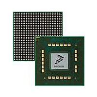
MPC8536DS Freescale Semiconductor, MPC8536DS Datasheet - Page 527

MPC8536DS
Manufacturer Part Number
MPC8536DS
Description
BOARD DEV SYSTEM MPC8536E
Manufacturer
Freescale Semiconductor
Series
PowerQUICC III™r
Type
MPUr
Datasheets
1.MPC8536EBVTAVLA.pdf
(127 pages)
2.MPC8536EBVTAVLA.pdf
(1706 pages)
3.MPC8536DS.pdf
(2 pages)
4.MPC8536DS.pdf
(126 pages)
Specifications of MPC8536DS
Contents
Board, Software and Documentation
Processor Series
MPC85xx
Core
e500
Data Bus Width
32 bit
Maximum Clock Frequency
667 MHz
Operating Supply Voltage
- 0.3 V to + 1.21 V
Maximum Operating Temperature
+ 105 C
Data Ram Size
32 KB
Interface Type
SPI, USB
Program Memory Type
DDR2, DDR3, SDRAM
Core Size
32 Bit
Program Memory Size
544KB
Cpu Speed
1.5GHz
Digital Ic Case Style
BGA
No. Of Pins
783
Supply Voltage Range
0.95V To 1.05V
Rohs Compliant
Yes
For Use With/related Products
MPC8536
Lead Free Status / RoHS Status
Lead free / RoHS Compliant
- MPC8536EBVTAVLA PDF datasheet
- MPC8536EBVTAVLA PDF datasheet #2
- MPC8536DS PDF datasheet #3
- MPC8536DS PDF datasheet #4
- Current page: 527 of 1706
- Download datasheet (15Mb)
before processing data. This mode is used to resume processing in an ARC4 session using a previously
computed S-box. In this case, the steps in the processing are as follows:
If the context registers are written during message processing or hen the PP bit is not set, a context error is
generated.
For more information about writing AFEU context through the input FIFO, see
“AFEU FIFOs.”
10.7.2.9.2
Once message processing is complete and the output data has been read, the AFEU S-box state can be read
out either through the context registers or through the output FIFO, as selected by the “dump context” (DC)
mode bit (see
Valid context data can only be read after AFEU has completed processing (as indicated by the done
interrupt, as reflected in the “DI” bit of the AFEU Status Register,
Register”). Reading context data before the module is done generates an error interrupt.
For more information about reading AFEU context through the output FIFO, see
“AFEU FIFOs.”
10.7.2.10 AFEU Key Registers
AFEU uses two write-only key registers to seed the initial permutation of the AFEU S-box, in conjunction
with the AFEU key size register. Any key data beyond the key size (specified in the key size register) is
ignored. AFEU permutes starting with the first byte of key register 0, and uses as many bytes from the two
key registers as necessary to complete the permutation. Reading either of these memory locations
generates an address error interrupt.
10.7.2.10.1 AFEU FIFOs
AFEU uses an input FIFO/output FIFO pair to hold data before and after the ciphering process. Normally,
the channels control all access to these FIFOs. For host-controlled operation, a write to anywhere in the
AFEU FIFO address space enqueues data to the AFEU input FIFO, and a read from anywhere in the AFEU
FIFO address space dequeues data from the AFEU output FIFO.
When context is written to the input FIFO (see
context write must be in the address range 3_8E00-3_8E07. Similarly, when context is read from the
output FIFO (see
address range 3_8E00-3_8E07. This causes any incomplete data word remaining in the output FIFO to be
cleared out so that the context can be read.
Freescale Semiconductor
1. Write the context to the AFEU through the context registers or through the input FIFO (as selected
2. Write the context length to the context/data length register (see
3. Write the message data size to the context/data register.
4. Write the message data.
by the CS mode bit).
Context/Data Size
Section 10.7.2.1, “AFEU Mode
Reading AFEU Context
Section 10.7.2.9.1, “Writing AFEU
MPC8536E PowerQUICC III Integrated Processor Reference Manual, Rev. 1
Register”).
Register”).
Section 10.7.2.9.1, “Writing AFEU
Context”), the first context read must be in the
Section 10.7.2.5, “AFEU Status
Section 10.7.2.3, “AFEU
Section 10.7.2.10.1,
Section 10.7.2.10.1,
Context”), the first
Security Engine (SEC) 3.0
10-97
Related parts for MPC8536DS
Image
Part Number
Description
Manufacturer
Datasheet
Request
R
Part Number:
Description:
Manufacturer:
Freescale Semiconductor, Inc
Datasheet:
Part Number:
Description:
Manufacturer:
Freescale Semiconductor, Inc
Datasheet:
Part Number:
Description:
Manufacturer:
Freescale Semiconductor, Inc
Datasheet:
Part Number:
Description:
Manufacturer:
Freescale Semiconductor, Inc
Datasheet:
Part Number:
Description:
Manufacturer:
Freescale Semiconductor, Inc
Datasheet:
Part Number:
Description:
Manufacturer:
Freescale Semiconductor, Inc
Datasheet:
Part Number:
Description:
Manufacturer:
Freescale Semiconductor, Inc
Datasheet:
Part Number:
Description:
Manufacturer:
Freescale Semiconductor, Inc
Datasheet:
Part Number:
Description:
Manufacturer:
Freescale Semiconductor, Inc
Datasheet:
Part Number:
Description:
Manufacturer:
Freescale Semiconductor, Inc
Datasheet:
Part Number:
Description:
Manufacturer:
Freescale Semiconductor, Inc
Datasheet:
Part Number:
Description:
Manufacturer:
Freescale Semiconductor, Inc
Datasheet:
Part Number:
Description:
Manufacturer:
Freescale Semiconductor, Inc
Datasheet:
Part Number:
Description:
Manufacturer:
Freescale Semiconductor, Inc
Datasheet:
Part Number:
Description:
Manufacturer:
Freescale Semiconductor, Inc
Datasheet:


