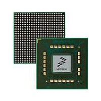
MPC8536DS Freescale Semiconductor, MPC8536DS Datasheet - Page 648

MPC8536DS
Manufacturer Part Number
MPC8536DS
Description
BOARD DEV SYSTEM MPC8536E
Manufacturer
Freescale Semiconductor
Series
PowerQUICC III™r
Type
MPUr
Datasheets
1.MPC8536EBVTAVLA.pdf
(127 pages)
2.MPC8536EBVTAVLA.pdf
(1706 pages)
3.MPC8536DS.pdf
(2 pages)
4.MPC8536DS.pdf
(126 pages)
Specifications of MPC8536DS
Contents
Board, Software and Documentation
Processor Series
MPC85xx
Core
e500
Data Bus Width
32 bit
Maximum Clock Frequency
667 MHz
Operating Supply Voltage
- 0.3 V to + 1.21 V
Maximum Operating Temperature
+ 105 C
Data Ram Size
32 KB
Interface Type
SPI, USB
Program Memory Type
DDR2, DDR3, SDRAM
Core Size
32 Bit
Program Memory Size
544KB
Cpu Speed
1.5GHz
Digital Ic Case Style
BGA
No. Of Pins
783
Supply Voltage Range
0.95V To 1.05V
Rohs Compliant
Yes
For Use With/related Products
MPC8536
Lead Free Status / RoHS Status
Lead free / RoHS Compliant
- MPC8536EBVTAVLA PDF datasheet
- MPC8536EBVTAVLA PDF datasheet #2
- MPC8536DS PDF datasheet #3
- MPC8536DS PDF datasheet #4
- Current page: 648 of 1706
- Download datasheet (15Mb)
Enhanced Local Bus Controller
13-6
LOE/LGPL2/
LWE[1:3]/
LCS[0:7]
LBS[1:3]
LGPL0/
LGPL1/
LGPL3/
LFWE/
LFCLE
Signal
LWE0/
LFALE
LFWP
LBS0,
LFRE
Table 13-2. Enhanced Local Bus Controller Detailed Signal Descriptions (continued)
I/O
O
O
O
O
O
O
Chip selects. Eight chip selects are provided that are mutually exclusive.
GPCM write enable 0/FCM write enable/UPM byte select 0. These signals select or validate each byte
lane of the data bus. For banks with port sizes of 32 bits (as set by BR n [PS]), all four signals are defined.
For a 16-bit port size, only bits 0–1 are defined; and for an 8-bit port size, bit 0 is the only defined signal.
The least-significant address bits of each access also determine which byte lanes are considered valid
for a given data transfer.
General purpose line 0/FCM command latch enable.
General-purpose line 1/FCM address latch enable.
GPCM output enable/General-purpose line 2/FCM read enable.
General-purpose line 3/FCM write protect.
Meaning
Meaning
Meaning
Meaning
Meaning
Meaning
MPC8536E PowerQUICC III Integrated Processor Reference Manual, Rev. 1
Timing Assertion/Negation—See
State
State
State
State
State
State
Asserted/Negated—Used to enable specific memory devices or peripherals connected to the
Asserted/Negated—For GPCM operation, LWE[0:3] assert for each byte lane enabled for
Asserted/Negated—In UPM mode, LGPL0 is one of six general purpose signals; it is driven
Asserted/Negated—In UPM mode, LGPL1 is one of six general purpose signals; it is driven
Asserted/Negated—Controls the output buffer of memory when accessing memory/devices in
Asserted/Negated—In UPM mode, LGPL3 is one of six general purpose signals; it is driven
eLBC. LCS[0:7] are provided on a per-bank basis with LCS0 corresponding to the chip
select for memory bank 0, which has the memory type and attributes defined by BR0 and
OR0.
writing.
LFWE enables command, address, and data writes to NAND Flash EEPROMs controlled
by FCM.
LBS[0:3] are programmable byte-select signals in UPM mode. See
“RAM
for details regarding the timing of LWE[0:3].
with a value programmed into the UPM array.
In FCM mode, LFCLE enables command cycles to NAND Flash EEPROMs.
with a value programmed into the UPM array.
In FCM mode, LFALE enables address cycles to NAND Flash EPROMs.
GPCM mode.
In UPM mode, LGPL2 is one of six general purpose signals; it is driven with a value
programmed into the UPM array.
LFRE enables data read cycles from NAND Flash EEPROMs controlled by FCM.
with a value programmed into the UPM array.
In FCM mode LFWP protects NAND Flash EEPROMs from accidental erasure and
programming when LFWP is asserted low—see
Register
Array,” for programming details about LBS[0:3].
(FMR),” for programming of FCM operations to control LFWP.
Section 13.4.2, “General-Purpose Chip-Select Machine
Description
Section 13.3.1.17, “Flash Mode
Freescale Semiconductor
Section 13.4.4.4,
(GPCM),”
Related parts for MPC8536DS
Image
Part Number
Description
Manufacturer
Datasheet
Request
R
Part Number:
Description:
Manufacturer:
Freescale Semiconductor, Inc
Datasheet:
Part Number:
Description:
Manufacturer:
Freescale Semiconductor, Inc
Datasheet:
Part Number:
Description:
Manufacturer:
Freescale Semiconductor, Inc
Datasheet:
Part Number:
Description:
Manufacturer:
Freescale Semiconductor, Inc
Datasheet:
Part Number:
Description:
Manufacturer:
Freescale Semiconductor, Inc
Datasheet:
Part Number:
Description:
Manufacturer:
Freescale Semiconductor, Inc
Datasheet:
Part Number:
Description:
Manufacturer:
Freescale Semiconductor, Inc
Datasheet:
Part Number:
Description:
Manufacturer:
Freescale Semiconductor, Inc
Datasheet:
Part Number:
Description:
Manufacturer:
Freescale Semiconductor, Inc
Datasheet:
Part Number:
Description:
Manufacturer:
Freescale Semiconductor, Inc
Datasheet:
Part Number:
Description:
Manufacturer:
Freescale Semiconductor, Inc
Datasheet:
Part Number:
Description:
Manufacturer:
Freescale Semiconductor, Inc
Datasheet:
Part Number:
Description:
Manufacturer:
Freescale Semiconductor, Inc
Datasheet:
Part Number:
Description:
Manufacturer:
Freescale Semiconductor, Inc
Datasheet:
Part Number:
Description:
Manufacturer:
Freescale Semiconductor, Inc
Datasheet:


