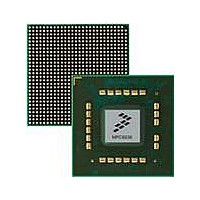
MPC8536DS Freescale Semiconductor, MPC8536DS Datasheet - Page 1109

MPC8536DS
Manufacturer Part Number
MPC8536DS
Description
BOARD DEV SYSTEM MPC8536E
Manufacturer
Freescale Semiconductor
Series
PowerQUICC III™r
Type
MPUr
Datasheets
1.MPC8536EBVTAVLA.pdf
(127 pages)
2.MPC8536EBVTAVLA.pdf
(1706 pages)
3.MPC8536DS.pdf
(2 pages)
4.MPC8536DS.pdf
(126 pages)
Specifications of MPC8536DS
Contents
Board, Software and Documentation
Processor Series
MPC85xx
Core
e500
Data Bus Width
32 bit
Maximum Clock Frequency
667 MHz
Operating Supply Voltage
- 0.3 V to + 1.21 V
Maximum Operating Temperature
+ 105 C
Data Ram Size
32 KB
Interface Type
SPI, USB
Program Memory Type
DDR2, DDR3, SDRAM
Core Size
32 Bit
Program Memory Size
544KB
Cpu Speed
1.5GHz
Digital Ic Case Style
BGA
No. Of Pins
783
Supply Voltage Range
0.95V To 1.05V
Rohs Compliant
Yes
For Use With/related Products
MPC8536
Lead Free Status / RoHS Status
Lead free / RoHS Compliant
- MPC8536EBVTAVLA PDF datasheet
- MPC8536EBVTAVLA PDF datasheet #2
- MPC8536DS PDF datasheet #3
- MPC8536DS PDF datasheet #4
- Current page: 1109 of 1706
- Download datasheet (15Mb)
The fields of the PCI Express configuration register are described in
17.3.3
17.3.3.1
The PCI Express PME and message detect register, shown in
PME events that are detected by the PCI Express controller. This register is a write-1-to-clear type register.
The fields of the PCI Express PME and message detect register are described in
Freescale Semiconductor
Offset 0x020
Reset
Reset
28–29
0–26
0–15
Bits
Bits
27
30
31
16
17
W
W w1c
R
R PTO
16
0
Name
Name
SAC
SCC
PTO
SP
—
—
—
—
PCI Express Power Management Event and Message Registers
Figure 17-7. PCI Express PME and Message Detect Register (PEX_PME_MES_DR)
—
17
PCI Express PME and Message Detect Register (PEX_PME_MES_DR)
Reserved
PME turn off. This bit indicates the detection of a PME_Turn_Off message. This bit is only valid in EP mode.
1 A PME_Turn_Off_message is detected
0 No PME_Turn_Off message detected
Reserved. Note that during normal operation, this bit may be set (falsely). The bit may be ignored and
cleared (w1c) without consequence.
Reserved
Sense ASPM Control. This bit controls the default value of ASPM of PEX Link Control Register’s bit 0. See
Section 17.3.9.11, “PCI Express Link Control Register—0x5C,”
Reserved
Slot Present. This bit controls the default value of the PCI Express capabilities register [slot] bit. See
Section 17.3.9.6, “PCI Express Capabilities Register—0x4E,”
Slot Clock Configuration. This bit controls the default value of the PCI Express link status register [SCC] bit.
See
ENL23
w1c
18
Section 17.3.9.12, “PCI Express Link Status Register—0x5E,”
MPC8536E PowerQUICC III Integrated Processor Reference Manual, Rev. 1
EXL23
w1c
19
Table 17-9. PEX_PME_MES_DR Field Descriptions
Table 17-8. PEX_CONFIG Field Descriptions
20
—
HRD
w1c
21
LDD
w1c
22
All zeros
All zeros
23
—
—
Description
Description
24
AION
w1c
Figure
25
for more information.
w1c
AIB
for more information.
26
Table
17-7, logs inbound messages and
for more information.
AIOF
w1c
17-8.
27
PCI Express Interface Controller
PION
Table
w1c
28
17-9.
w1c
PIB
29
PIOF
w1c
Access: w1c
30
ABP
w1c
17-13
15
31
Related parts for MPC8536DS
Image
Part Number
Description
Manufacturer
Datasheet
Request
R
Part Number:
Description:
Manufacturer:
Freescale Semiconductor, Inc
Datasheet:
Part Number:
Description:
Manufacturer:
Freescale Semiconductor, Inc
Datasheet:
Part Number:
Description:
Manufacturer:
Freescale Semiconductor, Inc
Datasheet:
Part Number:
Description:
Manufacturer:
Freescale Semiconductor, Inc
Datasheet:
Part Number:
Description:
Manufacturer:
Freescale Semiconductor, Inc
Datasheet:
Part Number:
Description:
Manufacturer:
Freescale Semiconductor, Inc
Datasheet:
Part Number:
Description:
Manufacturer:
Freescale Semiconductor, Inc
Datasheet:
Part Number:
Description:
Manufacturer:
Freescale Semiconductor, Inc
Datasheet:
Part Number:
Description:
Manufacturer:
Freescale Semiconductor, Inc
Datasheet:
Part Number:
Description:
Manufacturer:
Freescale Semiconductor, Inc
Datasheet:
Part Number:
Description:
Manufacturer:
Freescale Semiconductor, Inc
Datasheet:
Part Number:
Description:
Manufacturer:
Freescale Semiconductor, Inc
Datasheet:
Part Number:
Description:
Manufacturer:
Freescale Semiconductor, Inc
Datasheet:
Part Number:
Description:
Manufacturer:
Freescale Semiconductor, Inc
Datasheet:
Part Number:
Description:
Manufacturer:
Freescale Semiconductor, Inc
Datasheet:


