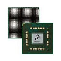
MPC8536DS Freescale Semiconductor, MPC8536DS Datasheet - Page 551

MPC8536DS
Manufacturer Part Number
MPC8536DS
Description
BOARD DEV SYSTEM MPC8536E
Manufacturer
Freescale Semiconductor
Series
PowerQUICC III™r
Type
MPUr
Datasheets
1.MPC8536EBVTAVLA.pdf
(127 pages)
2.MPC8536EBVTAVLA.pdf
(1706 pages)
3.MPC8536DS.pdf
(2 pages)
4.MPC8536DS.pdf
(126 pages)
Specifications of MPC8536DS
Contents
Board, Software and Documentation
Processor Series
MPC85xx
Core
e500
Data Bus Width
32 bit
Maximum Clock Frequency
667 MHz
Operating Supply Voltage
- 0.3 V to + 1.21 V
Maximum Operating Temperature
+ 105 C
Data Ram Size
32 KB
Interface Type
SPI, USB
Program Memory Type
DDR2, DDR3, SDRAM
Core Size
32 Bit
Program Memory Size
544KB
Cpu Speed
1.5GHz
Digital Ic Case Style
BGA
No. Of Pins
783
Supply Voltage Range
0.95V To 1.05V
Rohs Compliant
Yes
For Use With/related Products
MPC8536
Lead Free Status / RoHS Status
Lead free / RoHS Compliant
- MPC8536EBVTAVLA PDF datasheet
- MPC8536EBVTAVLA PDF datasheet #2
- MPC8536DS PDF datasheet #3
- MPC8536DS PDF datasheet #4
- Current page: 551 of 1706
- Download datasheet (15Mb)
For direct access mode f9 operations, assertion of PE enables f9 algorithm-specified padding per the value
in the data size register. If this direct access mode operation includes the final message block, then PE must
be set in the KEU mode register as follows:
10.7.5.4
The KEU reset control register, shown in
by the three self-clearing bits.
Table 10-54
Freescale Semiconductor
0–60
Bits
61
•
•
Reset
Field
Addr
R/W
Name
PE = 0: The KEU does not perform padding. For the KEU to perform the correct computation, the
last block of the message provided must be a complete 64-bit block, and the value written into the
KEU data size register must indicate a multiple of 64 bits.
PE = 1: The KEU pads the final 64 bits of the message as specified in the 3GPP f9 algorithm. The
communication direction (CD) bit (see
and ‘1’ is appended to the end of the message. The result is zero-padded to 64 bits.
For example, if the last block is xF81A_0000_0000_0000 (big endian) and data size contains 0x0F
(15 bits = 1 byte + 7 bits), the word (0xF81A = 1111_1000_0001_1010), the most-significant 15
bits (underlined) are padded left to right as
1111_1000_0001_101$_1000_0000_0000_0000_0000_0000_0000_0000_0000_0000_0000_000
0, where $ is the value of the CD bit in the mode register.
CLI
—
describes the KEU reset control register fields.
KEU Reset Control Register (KEURCR)
0
Reserved
Clear Interrupts.
Setting this bit causes the KEU interrupt signals—DONE and ERROR—to be reset. It further resets the state
of the KEU interrupt status register.
0 Normal operation
1 Clear interrupts and the KEU interrupt status register
MPC8536E PowerQUICC III Integrated Processor Reference Manual, Rev. 1
Table 10-54. KEU Reset Control Register Field Descriptions
Figure 10-67. KEU Reset Control Register
Figure
Table 10-58
—
10-67, allows three levels of reset of the KEU, as defined
KEU 0xE018
Description
R/W
0
for KEU IV_1 Register Fields Description)
60
Security Engine (SEC) 3.0
CLI
61
RI
62
SR
63
10-121
Related parts for MPC8536DS
Image
Part Number
Description
Manufacturer
Datasheet
Request
R
Part Number:
Description:
Manufacturer:
Freescale Semiconductor, Inc
Datasheet:
Part Number:
Description:
Manufacturer:
Freescale Semiconductor, Inc
Datasheet:
Part Number:
Description:
Manufacturer:
Freescale Semiconductor, Inc
Datasheet:
Part Number:
Description:
Manufacturer:
Freescale Semiconductor, Inc
Datasheet:
Part Number:
Description:
Manufacturer:
Freescale Semiconductor, Inc
Datasheet:
Part Number:
Description:
Manufacturer:
Freescale Semiconductor, Inc
Datasheet:
Part Number:
Description:
Manufacturer:
Freescale Semiconductor, Inc
Datasheet:
Part Number:
Description:
Manufacturer:
Freescale Semiconductor, Inc
Datasheet:
Part Number:
Description:
Manufacturer:
Freescale Semiconductor, Inc
Datasheet:
Part Number:
Description:
Manufacturer:
Freescale Semiconductor, Inc
Datasheet:
Part Number:
Description:
Manufacturer:
Freescale Semiconductor, Inc
Datasheet:
Part Number:
Description:
Manufacturer:
Freescale Semiconductor, Inc
Datasheet:
Part Number:
Description:
Manufacturer:
Freescale Semiconductor, Inc
Datasheet:
Part Number:
Description:
Manufacturer:
Freescale Semiconductor, Inc
Datasheet:
Part Number:
Description:
Manufacturer:
Freescale Semiconductor, Inc
Datasheet:


