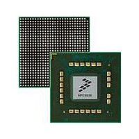
MPC8536DS Freescale Semiconductor, MPC8536DS Datasheet - Page 685

MPC8536DS
Manufacturer Part Number
MPC8536DS
Description
BOARD DEV SYSTEM MPC8536E
Manufacturer
Freescale Semiconductor
Series
PowerQUICC III™r
Type
MPUr
Datasheets
1.MPC8536EBVTAVLA.pdf
(127 pages)
2.MPC8536EBVTAVLA.pdf
(1706 pages)
3.MPC8536DS.pdf
(2 pages)
4.MPC8536DS.pdf
(126 pages)
Specifications of MPC8536DS
Contents
Board, Software and Documentation
Processor Series
MPC85xx
Core
e500
Data Bus Width
32 bit
Maximum Clock Frequency
667 MHz
Operating Supply Voltage
- 0.3 V to + 1.21 V
Maximum Operating Temperature
+ 105 C
Data Ram Size
32 KB
Interface Type
SPI, USB
Program Memory Type
DDR2, DDR3, SDRAM
Core Size
32 Bit
Program Memory Size
544KB
Cpu Speed
1.5GHz
Digital Ic Case Style
BGA
No. Of Pins
783
Supply Voltage Range
0.95V To 1.05V
Rohs Compliant
Yes
For Use With/related Products
MPC8536
Lead Free Status / RoHS Status
Lead free / RoHS Compliant
- MPC8536EBVTAVLA PDF datasheet
- MPC8536EBVTAVLA PDF datasheet #2
- MPC8536DS PDF datasheet #3
- MPC8536DS PDF datasheet #4
- Current page: 685 of 1706
- Download datasheet (15Mb)
Each memory bank (chip select) can be assigned to any of these three types of machines through the
machine select bits of the base register for that bank (BRn[MSEL]), as illustrated in
match occurs, the corresponding machine (GPCM, FCM, or UPM) then takes ownership of the external
signals that control the access and maintains control until the transaction ends.
13.4.1
The following subsections describe the basic architecture of the eLBC.
13.4.1.1
The defined base addresses are written to the BRn registers, while the corresponding address masks are
written to the ORn registers. Each time a local bus access is requested, the internal transaction address is
compared with each bank. Addresses are decoded by comparing the 17 MSBs of the address, masked by
ORn[AM], with the base address for each bank (BRn[BA]). If a match is found on a memory controller
bank, the attributes defined in the BRn and ORn for that bank are used to control the memory access. If a
match is found in more than one bank, the lowest-numbered bank handles the memory access (that is, bank
0 has priority over bank 1).
13.4.1.2
The local bus uses a multiplexed address/data bus. Therefore the eLBC must distinguish between address
and data phases, which take place on the same bus (LAD pins). The LALE signal, when asserted, signifies
an address phase during which the eLBC drives the memory address on the LAD pins. An external address
Freescale Semiconductor
Basic Architecture
Address and Address Space Checking
External Address Latch Enable Signal (LALE)
Bank Select
Comparator
MPC8536E PowerQUICC III Integrated Processor Reference Manual, Rev. 1
Address
Figure 13-29. Basic Operation of Memory Controllers in the eLBC
MSEL
Field
32-bit Physical
RAM Address (A)
32-bit System
Address
Internal Memory Access Request Select
UPM A/B/C
Signals Timing Generator
External Signals
FCM buffer
RAM
FCM
GPCM
Enhanced Local Bus Controller
Figure
13-29. If a bank
13-43
Related parts for MPC8536DS
Image
Part Number
Description
Manufacturer
Datasheet
Request
R
Part Number:
Description:
Manufacturer:
Freescale Semiconductor, Inc
Datasheet:
Part Number:
Description:
Manufacturer:
Freescale Semiconductor, Inc
Datasheet:
Part Number:
Description:
Manufacturer:
Freescale Semiconductor, Inc
Datasheet:
Part Number:
Description:
Manufacturer:
Freescale Semiconductor, Inc
Datasheet:
Part Number:
Description:
Manufacturer:
Freescale Semiconductor, Inc
Datasheet:
Part Number:
Description:
Manufacturer:
Freescale Semiconductor, Inc
Datasheet:
Part Number:
Description:
Manufacturer:
Freescale Semiconductor, Inc
Datasheet:
Part Number:
Description:
Manufacturer:
Freescale Semiconductor, Inc
Datasheet:
Part Number:
Description:
Manufacturer:
Freescale Semiconductor, Inc
Datasheet:
Part Number:
Description:
Manufacturer:
Freescale Semiconductor, Inc
Datasheet:
Part Number:
Description:
Manufacturer:
Freescale Semiconductor, Inc
Datasheet:
Part Number:
Description:
Manufacturer:
Freescale Semiconductor, Inc
Datasheet:
Part Number:
Description:
Manufacturer:
Freescale Semiconductor, Inc
Datasheet:
Part Number:
Description:
Manufacturer:
Freescale Semiconductor, Inc
Datasheet:
Part Number:
Description:
Manufacturer:
Freescale Semiconductor, Inc
Datasheet:


