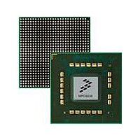
MPC8536DS Freescale Semiconductor, MPC8536DS Datasheet - Page 710

MPC8536DS
Manufacturer Part Number
MPC8536DS
Description
BOARD DEV SYSTEM MPC8536E
Manufacturer
Freescale Semiconductor
Series
PowerQUICC III™r
Type
MPUr
Datasheets
1.MPC8536EBVTAVLA.pdf
(127 pages)
2.MPC8536EBVTAVLA.pdf
(1706 pages)
3.MPC8536DS.pdf
(2 pages)
4.MPC8536DS.pdf
(126 pages)
Specifications of MPC8536DS
Contents
Board, Software and Documentation
Processor Series
MPC85xx
Core
e500
Data Bus Width
32 bit
Maximum Clock Frequency
667 MHz
Operating Supply Voltage
- 0.3 V to + 1.21 V
Maximum Operating Temperature
+ 105 C
Data Ram Size
32 KB
Interface Type
SPI, USB
Program Memory Type
DDR2, DDR3, SDRAM
Core Size
32 Bit
Program Memory Size
544KB
Cpu Speed
1.5GHz
Digital Ic Case Style
BGA
No. Of Pins
783
Supply Voltage Range
0.95V To 1.05V
Rohs Compliant
Yes
For Use With/related Products
MPC8536
Lead Free Status / RoHS Status
Lead free / RoHS Compliant
- MPC8536EBVTAVLA PDF datasheet
- MPC8536EBVTAVLA PDF datasheet #2
- MPC8536DS PDF datasheet #3
- MPC8536DS PDF datasheet #4
- Current page: 710 of 1706
- Download datasheet (15Mb)
Enhanced Local Bus Controller
13.4.3.3
If BRn[MSEL] selects the FCM, the attributes for the memory cycle are taken from ORn. These attributes
include the CSCT, CST, CHT, RST, SCY, TRLX, and EHTR fields.
13.4.3.3.1
The timing of LCSn assertion in FCM mode is illustrated by the timing diagram in
asserted immediately following LALE negation, and remains asserted until the last instruction in FIR has
completed. The delay, t
instruction is controlled by ORn[CSCT] and ORn[TRLX], as shown in
be set in accordance with the NAND Flash EEPROM chip-select to WE set-up time specification.
13.4.3.3.2
The FCM command (CM0–CM3, CW0, CW1), address (CA, PA, UA), and data write (WB, WS)
instructions all share the same basic timing attributes. Assertion of LFWE initiates transfer via LAD[0:7],
and the options in ORn for FCM mode establish the set-up, hold, and wait state timings with respect to
LFWE, as shown in
13-68
LCLK
(unused)
LFCLE/
LFALE
LFWE
LAD[0:7]
TA
FCM Signal Timing
FCM Chip-Select Timing
FCM Command, Address, and Write Data Timing
Notes:
Figure 13-54. Timing of FCM Command/Address and Write Data Cycles
MPC8536E PowerQUICC III Integrated Processor Reference Manual, Rev. 1
Figure
CSCT
t
t
t
CST
CHT
ADL
Table 13-35. FCM Chip-Select to First Command Timing
ORn[TRLX] ORn[CSCT] LCS n to First Command Delay
13-54.
= Command/address to write data delay.
= Command to LFWE set-up time.
= Command to LFWE hold time.
, between LCSn assertion and commencement of the first NAND Flash
command/address
t
write cycle #1
CST
0
0
1
1
(for TRLX = 0, CHT = 0, CST = 1, SCY = 1)
t
t
WP
t
WC
WS
0
1
0
1
1 LCLK clock cycle
4 LCLK clock cycles
2 LCLK clock cycles
8 LCLK clock cycles
t
t
CHT
ADL
t
t
t
WP
WS
WC
= LFWE pulse time, driven low.
= Command wait state time.
= Command cycle time.
Table
write cycle #2
write data
13-35. ORn[CSCT] should
Figure
Freescale Semiconductor
13-47. LCSn is
Related parts for MPC8536DS
Image
Part Number
Description
Manufacturer
Datasheet
Request
R
Part Number:
Description:
Manufacturer:
Freescale Semiconductor, Inc
Datasheet:
Part Number:
Description:
Manufacturer:
Freescale Semiconductor, Inc
Datasheet:
Part Number:
Description:
Manufacturer:
Freescale Semiconductor, Inc
Datasheet:
Part Number:
Description:
Manufacturer:
Freescale Semiconductor, Inc
Datasheet:
Part Number:
Description:
Manufacturer:
Freescale Semiconductor, Inc
Datasheet:
Part Number:
Description:
Manufacturer:
Freescale Semiconductor, Inc
Datasheet:
Part Number:
Description:
Manufacturer:
Freescale Semiconductor, Inc
Datasheet:
Part Number:
Description:
Manufacturer:
Freescale Semiconductor, Inc
Datasheet:
Part Number:
Description:
Manufacturer:
Freescale Semiconductor, Inc
Datasheet:
Part Number:
Description:
Manufacturer:
Freescale Semiconductor, Inc
Datasheet:
Part Number:
Description:
Manufacturer:
Freescale Semiconductor, Inc
Datasheet:
Part Number:
Description:
Manufacturer:
Freescale Semiconductor, Inc
Datasheet:
Part Number:
Description:
Manufacturer:
Freescale Semiconductor, Inc
Datasheet:
Part Number:
Description:
Manufacturer:
Freescale Semiconductor, Inc
Datasheet:
Part Number:
Description:
Manufacturer:
Freescale Semiconductor, Inc
Datasheet:


