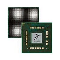
MPC8536DS Freescale Semiconductor, MPC8536DS Datasheet - Page 237

MPC8536DS
Manufacturer Part Number
MPC8536DS
Description
BOARD DEV SYSTEM MPC8536E
Manufacturer
Freescale Semiconductor
Series
PowerQUICC III™r
Type
MPUr
Datasheets
1.MPC8536EBVTAVLA.pdf
(127 pages)
2.MPC8536EBVTAVLA.pdf
(1706 pages)
3.MPC8536DS.pdf
(2 pages)
4.MPC8536DS.pdf
(126 pages)
Specifications of MPC8536DS
Contents
Board, Software and Documentation
Processor Series
MPC85xx
Core
e500
Data Bus Width
32 bit
Maximum Clock Frequency
667 MHz
Operating Supply Voltage
- 0.3 V to + 1.21 V
Maximum Operating Temperature
+ 105 C
Data Ram Size
32 KB
Interface Type
SPI, USB
Program Memory Type
DDR2, DDR3, SDRAM
Core Size
32 Bit
Program Memory Size
544KB
Cpu Speed
1.5GHz
Digital Ic Case Style
BGA
No. Of Pins
783
Supply Voltage Range
0.95V To 1.05V
Rohs Compliant
Yes
For Use With/related Products
MPC8536
Lead Free Status / RoHS Status
Lead free / RoHS Compliant
- MPC8536EBVTAVLA PDF datasheet
- MPC8536EBVTAVLA PDF datasheet #2
- MPC8536DS PDF datasheet #3
- MPC8536DS PDF datasheet #4
- Current page: 237 of 1706
- Download datasheet (15Mb)
6.3.1.3.2
The L2 memory-mapped SRAM base address registers extended address (L2SRBAREAn), shown in
Figure
Table 6-9
6.3.1.4
L2 error detection, reporting, and injection allow flexible handling of ECC and parity errors in the L2 data
and tag arrays. When the device detects an L2 error, the appropriate bit in the error detect register
(L2ERRDET) is set. Error detection is disabled by setting the corresponding bit in the error disable register
(L2ERRDIS).
The address and attributes of the first detected error are also saved in the error capture registers
(L2ERRADDR, L2ERRATTR, L2CAPTDATAHI, L2CAPTDATALO, and L2CAPTACC). Subsequent
errors set error bits in the error detection registers, but information is saved only for the first one. Error
reporting (by generating an interrupt) is enabled by setting the corresponding bit in the error interrupt
enable register (L2ERRINTEN). Note that the error detect bit is set regardless of the state of the interrupt
enable bit. When an error is detected, if error detection is enabled the L2 cache/SRAM always asserts an
internal error signal with read data to prevent the L1 caches and architectural registers from being loaded
with corrupt data. If error detection is disabled, the detected error bit is not set and no internal signal is
asserted.
The L2 error detect register (L2ERRDET) is implemented as a bit-reset type register. Reading from this
register occurs normally; however, write operations can clear but not set bits. A bit is cleared whenever the
register is written and the data in the corresponding bit location is a 1. For example, to clear bit 6 and not
affect any other bits in the register, the value 0x0200_0000 is written to the register.
Note that in SRAM mode, if a non–cache-line read or write transaction is not preceded by a cache-line
write, an ECC error occurs; such a non–cache-line write transaction cannot be allocated in the L2.
Freescale Semiconductor
Offset 0x2_0104
Reset
28–31
0–27
Bits
W
R
6-12, contain the upper 4 bits of the L2 cache SRAM base address.
0x2_010C
0
Figure 6-12. L2 Memory-Mapped SRAM Base Address Registers Extended Address 0–1
describes the fields of L2SRBAREAn.
ADDR
Name
—
L2 Error Registers
L2 Memory-Mapped SRAM Base Address Registers Extended Address 0–1
(L2SRBAREA n )
MPC8536E PowerQUICC III Integrated Processor Reference Manual, Rev. 1
Reserved
base address are contained in L2SRBAR n [ADDR].
Contains the upper 4 bits of the L2 cache SRAM base address. Note that the 18 low-order bits of the
Table 6-9. L2SRBAREA n Field Descriptions
(L2SRBAREA n )
—
All zeros
Description
L2 Look-Aside Cache/SRAM
Access: Read/Write
27 28
ADDR
6-17
31
Related parts for MPC8536DS
Image
Part Number
Description
Manufacturer
Datasheet
Request
R
Part Number:
Description:
Manufacturer:
Freescale Semiconductor, Inc
Datasheet:
Part Number:
Description:
Manufacturer:
Freescale Semiconductor, Inc
Datasheet:
Part Number:
Description:
Manufacturer:
Freescale Semiconductor, Inc
Datasheet:
Part Number:
Description:
Manufacturer:
Freescale Semiconductor, Inc
Datasheet:
Part Number:
Description:
Manufacturer:
Freescale Semiconductor, Inc
Datasheet:
Part Number:
Description:
Manufacturer:
Freescale Semiconductor, Inc
Datasheet:
Part Number:
Description:
Manufacturer:
Freescale Semiconductor, Inc
Datasheet:
Part Number:
Description:
Manufacturer:
Freescale Semiconductor, Inc
Datasheet:
Part Number:
Description:
Manufacturer:
Freescale Semiconductor, Inc
Datasheet:
Part Number:
Description:
Manufacturer:
Freescale Semiconductor, Inc
Datasheet:
Part Number:
Description:
Manufacturer:
Freescale Semiconductor, Inc
Datasheet:
Part Number:
Description:
Manufacturer:
Freescale Semiconductor, Inc
Datasheet:
Part Number:
Description:
Manufacturer:
Freescale Semiconductor, Inc
Datasheet:
Part Number:
Description:
Manufacturer:
Freescale Semiconductor, Inc
Datasheet:
Part Number:
Description:
Manufacturer:
Freescale Semiconductor, Inc
Datasheet:


