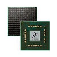
MPC8536DS Freescale Semiconductor, MPC8536DS Datasheet - Page 357

MPC8536DS
Manufacturer Part Number
MPC8536DS
Description
BOARD DEV SYSTEM MPC8536E
Manufacturer
Freescale Semiconductor
Series
PowerQUICC III™r
Type
MPUr
Datasheets
1.MPC8536EBVTAVLA.pdf
(127 pages)
2.MPC8536EBVTAVLA.pdf
(1706 pages)
3.MPC8536DS.pdf
(2 pages)
4.MPC8536DS.pdf
(126 pages)
Specifications of MPC8536DS
Contents
Board, Software and Documentation
Processor Series
MPC85xx
Core
e500
Data Bus Width
32 bit
Maximum Clock Frequency
667 MHz
Operating Supply Voltage
- 0.3 V to + 1.21 V
Maximum Operating Temperature
+ 105 C
Data Ram Size
32 KB
Interface Type
SPI, USB
Program Memory Type
DDR2, DDR3, SDRAM
Core Size
32 Bit
Program Memory Size
544KB
Cpu Speed
1.5GHz
Digital Ic Case Style
BGA
No. Of Pins
783
Supply Voltage Range
0.95V To 1.05V
Rohs Compliant
Yes
For Use With/related Products
MPC8536
Lead Free Status / RoHS Status
Lead free / RoHS Compliant
- MPC8536EBVTAVLA PDF datasheet
- MPC8536EBVTAVLA PDF datasheet #2
- MPC8536DS PDF datasheet #3
- MPC8536DS PDF datasheet #4
- Current page: 357 of 1706
- Download datasheet (15Mb)
8.5.9
Transfers to and from memory are always performed in four- or eight-beat bursts (four beats = 32 bytes
when a 64-bit bus is used). For transfer sizes other than four or eight beats, the data transfers are still
operated as four- or eight-beat bursts. If ECC is enabled and either the access is not doubleword aligned
or the size is not a multiple of a doubleword, a full read-modify-write is performed for a write to SDRAM.
If ECC is disabled or both the access is doubleword aligned with a size that is a multiple of a doubleword,
the data masks (MDM[0:8] (MDM[0:4] for 32-bit bus) can be used to prevent the writing of unwanted data
to SDRAM. The DDR memory controller also uses data masks to prevent all unintended full double words
from writing to SDRAM. For example, if a write transaction is desired with a size of one double word
(8 bytes), then the second, third, and fourth beats of data are not written to DRAM.
Table 8-64
the possible transfer sizes with each of the possible starting double-word offsets. All underlined
double-word offsets are valid for the transaction.
8.5.10
The DDR memory controller supports an open/closed page mode with an allowable open page for each
logical bank of DRAM used. In closed page mode for DDR SDRAMs, the DDR memory controller uses
the SDRAM auto-precharge feature, which allows the controller to indicate that the page must be
automatically closed by the DDR SDRAM after the READ or WRITE access. This is performed using
MA[10] of the address during the COMMAND phase of the access to enable auto-precharge.
Auto-precharge is non-persistent in that it is either enabled or disabled for each individual READ or
WRITE command. It can, however, be enabled or disabled separately for each chip select.
When the DDR memory controller operates in open page mode, it retains the currently active SDRAM
page by not issuing a precharge command. The page remains opens until one of the following conditions
occurs:
Freescale Semiconductor
•
•
Refresh interval is met.
The user-programmable DDR_SDRAM_INTERVAL[BSTOPRE] value is exceeded.
lists the data beat sequencing to and from the DDR SDRAM and the data queues for each of
DDR Data Beat Ordering
Page Mode and Logical Bank Retention
1
All underlined Double-word offsets are valid for the transaction. All writes are aligned to
double-word 0 for DDR3 memories.
2 double words
3 double words
1 double word
Transfer Size
MPC8536E PowerQUICC III Integrated Processor Reference Manual, Rev. 1
Table 8-64. Memory Controller–Data Beat Ordering
Starting Double-Word Offset
0
1
2
3
0
1
2
0
1
Double-Word Sequence
DRAM and Queues
0 - 1 - 2 - 3
1 - 2 - 3 - 0
2 - 3 - 0 - 1
3 - 0 - 1 - 2
0 - 1 - 2 - 3
1 - 2 - 3 - 0
2 - 3 - 0 - 1
0 - 1 - 2 - 3
1 - 2 - 3 - 0
1
to/from
DDR Memory Controller
8-83
Related parts for MPC8536DS
Image
Part Number
Description
Manufacturer
Datasheet
Request
R
Part Number:
Description:
Manufacturer:
Freescale Semiconductor, Inc
Datasheet:
Part Number:
Description:
Manufacturer:
Freescale Semiconductor, Inc
Datasheet:
Part Number:
Description:
Manufacturer:
Freescale Semiconductor, Inc
Datasheet:
Part Number:
Description:
Manufacturer:
Freescale Semiconductor, Inc
Datasheet:
Part Number:
Description:
Manufacturer:
Freescale Semiconductor, Inc
Datasheet:
Part Number:
Description:
Manufacturer:
Freescale Semiconductor, Inc
Datasheet:
Part Number:
Description:
Manufacturer:
Freescale Semiconductor, Inc
Datasheet:
Part Number:
Description:
Manufacturer:
Freescale Semiconductor, Inc
Datasheet:
Part Number:
Description:
Manufacturer:
Freescale Semiconductor, Inc
Datasheet:
Part Number:
Description:
Manufacturer:
Freescale Semiconductor, Inc
Datasheet:
Part Number:
Description:
Manufacturer:
Freescale Semiconductor, Inc
Datasheet:
Part Number:
Description:
Manufacturer:
Freescale Semiconductor, Inc
Datasheet:
Part Number:
Description:
Manufacturer:
Freescale Semiconductor, Inc
Datasheet:
Part Number:
Description:
Manufacturer:
Freescale Semiconductor, Inc
Datasheet:
Part Number:
Description:
Manufacturer:
Freescale Semiconductor, Inc
Datasheet:


