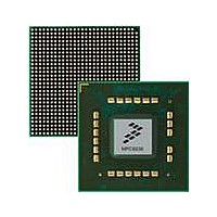
MPC8536DS Freescale Semiconductor, MPC8536DS Datasheet - Page 1198

MPC8536DS
Manufacturer Part Number
MPC8536DS
Description
BOARD DEV SYSTEM MPC8536E
Manufacturer
Freescale Semiconductor
Series
PowerQUICC III™r
Type
MPUr
Datasheets
1.MPC8536EBVTAVLA.pdf
(127 pages)
2.MPC8536EBVTAVLA.pdf
(1706 pages)
3.MPC8536DS.pdf
(2 pages)
4.MPC8536DS.pdf
(126 pages)
Specifications of MPC8536DS
Contents
Board, Software and Documentation
Processor Series
MPC85xx
Core
e500
Data Bus Width
32 bit
Maximum Clock Frequency
667 MHz
Operating Supply Voltage
- 0.3 V to + 1.21 V
Maximum Operating Temperature
+ 105 C
Data Ram Size
32 KB
Interface Type
SPI, USB
Program Memory Type
DDR2, DDR3, SDRAM
Core Size
32 Bit
Program Memory Size
544KB
Cpu Speed
1.5GHz
Digital Ic Case Style
BGA
No. Of Pins
783
Supply Voltage Range
0.95V To 1.05V
Rohs Compliant
Yes
For Use With/related Products
MPC8536
Lead Free Status / RoHS Status
Lead free / RoHS Compliant
- MPC8536EBVTAVLA PDF datasheet
- MPC8536EBVTAVLA PDF datasheet #2
- MPC8536DS PDF datasheet #3
- MPC8536DS PDF datasheet #4
- Current page: 1198 of 1706
- Download datasheet (15Mb)
PCI Express Interface Controller
Note that lane reversal is only effective for devices that use the full 8 lanes. That is, if a x4 device is
connected to lanes 0–3 and the link training fails without lane reversal, the lane reversal causes the link to
attempt connection on lanes 7–4 which would be impossible.
17.4.1.4
In general, transactions are serviced in the order that they are received. However, transactions can be
reordered as they are sent due to a stalled condition such as a full internal buffer. The following are the
ordering rules for sending the next outstanding request:
17.4.1.5
A PCI Express memory transaction can address a 32- or 64-bit memory space. The FMT[0] field in the
PCI Express TLP header for a 32-bit address packet is 0; a 64-bit address packet has a FMT[0] = 1. The
PCI Express TLP header for a memory read transaction has TYPE[4:0] = 00000 and FMT[1] = 0. A
memory write transaction has TYPE[4:0] = 00000 and FMT[1] = 1. As an initiator, the controller is
capable of sending 32- or 64-bit memory packets. Any transaction from the internal platform that (after
passing through the translation mechanism) has a translated address greater than 4G is sent as a 64-bit
memory packet. Otherwise, a 32-bit memory packet is sent. As a target device, the controller is capable of
decoding 32- or 64-bit memory packets. This is done through two 32-bit inbound windows and two 64-bit
inbound windows. All inbound addresses are translated to 36-bit internal platform addresses.
17.4.1.6
The controller does not support I/O transactions as a target. As an initiator, the controller can send I/O
transactions in RC mode only. This can be done by programming one of the outbound translation window’s
attribute to send I/O transactions. All I/O transactions only access 32-bit address I/O space. The PCI
Express TLP header for an I/O read transaction has TYPE[4:0] = 00010 and FMT[1] = 0. The PCI Express
TLP header for an I/O write transaction has TYPE[4:0] = 00010 and FMT[1] = 1.
17-102
•
•
•
x4 link with lane reversal
x2 link with lane reversal
x1 link with lane reversal
Note: The numbers shown in this table (0–7) are the lane numbers assigned to each lane as a result of link
A posted request can and bypasses all other transactions except another posted request.
A completion can and only bypasses non-posted. It can and bypasses posted requests only if the
relaxed ordering (RO) bit is set.
A non-posted request cannot bypass posted or other non-posted requests, but it can bypass a
completion if the relaxed ordering (RO) bit is set.
Link Configuration
initialization and configuration.
— indicates that the lane is not part of the configured link.
Transaction Ordering Rules
Memory Space Addressing
I/O Space Addressing
Table 17-120. Lane Assignment With and Without Lane Reversal (continued)
MPC8536E PowerQUICC III Integrated Processor Reference Manual, Rev. 1
Lane 0
—
—
—
Lane 1
—
—
—
Lane 2
—
—
—
Lane 3
—
—
—
Lane 4
—
—
3
Lane 5
—
—
2
Freescale Semiconductor
Lane 6
—
1
1
Lane 7
0
0
0
Related parts for MPC8536DS
Image
Part Number
Description
Manufacturer
Datasheet
Request
R
Part Number:
Description:
Manufacturer:
Freescale Semiconductor, Inc
Datasheet:
Part Number:
Description:
Manufacturer:
Freescale Semiconductor, Inc
Datasheet:
Part Number:
Description:
Manufacturer:
Freescale Semiconductor, Inc
Datasheet:
Part Number:
Description:
Manufacturer:
Freescale Semiconductor, Inc
Datasheet:
Part Number:
Description:
Manufacturer:
Freescale Semiconductor, Inc
Datasheet:
Part Number:
Description:
Manufacturer:
Freescale Semiconductor, Inc
Datasheet:
Part Number:
Description:
Manufacturer:
Freescale Semiconductor, Inc
Datasheet:
Part Number:
Description:
Manufacturer:
Freescale Semiconductor, Inc
Datasheet:
Part Number:
Description:
Manufacturer:
Freescale Semiconductor, Inc
Datasheet:
Part Number:
Description:
Manufacturer:
Freescale Semiconductor, Inc
Datasheet:
Part Number:
Description:
Manufacturer:
Freescale Semiconductor, Inc
Datasheet:
Part Number:
Description:
Manufacturer:
Freescale Semiconductor, Inc
Datasheet:
Part Number:
Description:
Manufacturer:
Freescale Semiconductor, Inc
Datasheet:
Part Number:
Description:
Manufacturer:
Freescale Semiconductor, Inc
Datasheet:
Part Number:
Description:
Manufacturer:
Freescale Semiconductor, Inc
Datasheet:


