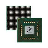
MPC8536DS Freescale Semiconductor, MPC8536DS Datasheet - Page 250

MPC8536DS
Manufacturer Part Number
MPC8536DS
Description
BOARD DEV SYSTEM MPC8536E
Manufacturer
Freescale Semiconductor
Series
PowerQUICC III™r
Type
MPUr
Datasheets
1.MPC8536EBVTAVLA.pdf
(127 pages)
2.MPC8536EBVTAVLA.pdf
(1706 pages)
3.MPC8536DS.pdf
(2 pages)
4.MPC8536DS.pdf
(126 pages)
Specifications of MPC8536DS
Contents
Board, Software and Documentation
Processor Series
MPC85xx
Core
e500
Data Bus Width
32 bit
Maximum Clock Frequency
667 MHz
Operating Supply Voltage
- 0.3 V to + 1.21 V
Maximum Operating Temperature
+ 105 C
Data Ram Size
32 KB
Interface Type
SPI, USB
Program Memory Type
DDR2, DDR3, SDRAM
Core Size
32 Bit
Program Memory Size
544KB
Cpu Speed
1.5GHz
Digital Ic Case Style
BGA
No. Of Pins
783
Supply Voltage Range
0.95V To 1.05V
Rohs Compliant
Yes
For Use With/related Products
MPC8536
Lead Free Status / RoHS Status
Lead free / RoHS Compliant
- MPC8536EBVTAVLA PDF datasheet
- MPC8536EBVTAVLA PDF datasheet #2
- MPC8536DS PDF datasheet #3
- MPC8536DS PDF datasheet #4
- Current page: 250 of 1706
- Download datasheet (15Mb)
L2 Look-Aside Cache/SRAM
coherency. Lines invalidated to satisfy coherency requirements cannot be reallocated by core requests
while the cache remains locked. The L2 cache can be unlocked by clearing L2CTL[L2IO] and/or
L2CTL[L2DO]. Note that L2CTL[L2DO] and L2CTL[L2IO] have no effect on cache external write
allocations or memory-mapped SRAM.
Note that this form of cache locking does not use the lock bits of the cache and cannot be cleared by
resetting the cache or lock bits.
6.7.2
A programmed memory range can be locked with a snoop write transaction that matches a cache external
write address range (specified by L2CEWARn/L2CEWAREAn and L2CEWCRn). There are no clearing
of locks through the programmed address ranges. Locks can be cleared using clear lock instructions,
flushes, read-and-clear-lock snoop (RWNITC with clear lock attribute), or flash clear locks.
6.7.3
Individual lines are locked when the L2 receives one of the following burst transactions:
Note that the core complex broadcasts these instructions to the L2 if the CT field in the instruction specifies
the L2 cache (CT = 1). When the L2 cache is specified, data is not placed in the L1, only the L2. If the L1
cache is specified (CT = 0), the L2 does not lock the line, and the data is placed in the L1 (and locked).
When the touch lock set L2 instruction (dcbtls or dcbtstls) hits are modified in the L1 cache, the modified
data is allocated into the L2 cache (and written back to main memory) and a data lock is set. The L1 line
state transitions to invalid.
Note that if the L2 receives a request to allocate and lock a line, but all lines in the selected way are locked,
the requested L2 line is not allocated and the L2 cache lock overflow bit (L2CTL[L2LO]) is set.
Lines invalidated to satisfy coherency requirements cannot be reallocated while the cache remains locked.
6.7.4
Individual locks in the L2 are cleared by a lock clear (icblc or dcblc, CT = 1) instruction. This directs the
L2 cache to clear a lock on that line if it hits in the L2 cache. Both data and instruction locks are cleared
by the icblc and dcblc instructions.
Note that the lock on a line is cleared if the line is invalidated by a snooped Flush transaction, and the line
in the cache is available for allocation of a new line of instruction or data unless the entire cache is locked.
6-30
•
•
•
•
•
icbtls (CT = 1)—Instruction Cache Block Touch and Lock Set instruction
dcbtls (CT = 1)—Data Cache Block Touch and Lock Set instruction
dcbtstls (CT = 1)—Data Cache Block Touch for Store and Lock Set instruction
Snoop burst write—If the address hits on a programmed cache external write space with the lock
attribute set, or if the write allocate transaction type is used
Snoop non-burst write—If the address hits on a programmed cache external write space with the
lock attribute set
Locking Programmed Memory Ranges
Locking Selected Lines
Clearing Locks on Selected Lines
MPC8536E PowerQUICC III Integrated Processor Reference Manual, Rev. 1
Freescale Semiconductor
Related parts for MPC8536DS
Image
Part Number
Description
Manufacturer
Datasheet
Request
R
Part Number:
Description:
Manufacturer:
Freescale Semiconductor, Inc
Datasheet:
Part Number:
Description:
Manufacturer:
Freescale Semiconductor, Inc
Datasheet:
Part Number:
Description:
Manufacturer:
Freescale Semiconductor, Inc
Datasheet:
Part Number:
Description:
Manufacturer:
Freescale Semiconductor, Inc
Datasheet:
Part Number:
Description:
Manufacturer:
Freescale Semiconductor, Inc
Datasheet:
Part Number:
Description:
Manufacturer:
Freescale Semiconductor, Inc
Datasheet:
Part Number:
Description:
Manufacturer:
Freescale Semiconductor, Inc
Datasheet:
Part Number:
Description:
Manufacturer:
Freescale Semiconductor, Inc
Datasheet:
Part Number:
Description:
Manufacturer:
Freescale Semiconductor, Inc
Datasheet:
Part Number:
Description:
Manufacturer:
Freescale Semiconductor, Inc
Datasheet:
Part Number:
Description:
Manufacturer:
Freescale Semiconductor, Inc
Datasheet:
Part Number:
Description:
Manufacturer:
Freescale Semiconductor, Inc
Datasheet:
Part Number:
Description:
Manufacturer:
Freescale Semiconductor, Inc
Datasheet:
Part Number:
Description:
Manufacturer:
Freescale Semiconductor, Inc
Datasheet:
Part Number:
Description:
Manufacturer:
Freescale Semiconductor, Inc
Datasheet:


