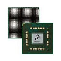
MPC8536DS Freescale Semiconductor, MPC8536DS Datasheet - Page 650

MPC8536DS
Manufacturer Part Number
MPC8536DS
Description
BOARD DEV SYSTEM MPC8536E
Manufacturer
Freescale Semiconductor
Series
PowerQUICC III™r
Type
MPUr
Datasheets
1.MPC8536EBVTAVLA.pdf
(127 pages)
2.MPC8536EBVTAVLA.pdf
(1706 pages)
3.MPC8536DS.pdf
(2 pages)
4.MPC8536DS.pdf
(126 pages)
Specifications of MPC8536DS
Contents
Board, Software and Documentation
Processor Series
MPC85xx
Core
e500
Data Bus Width
32 bit
Maximum Clock Frequency
667 MHz
Operating Supply Voltage
- 0.3 V to + 1.21 V
Maximum Operating Temperature
+ 105 C
Data Ram Size
32 KB
Interface Type
SPI, USB
Program Memory Type
DDR2, DDR3, SDRAM
Core Size
32 Bit
Program Memory Size
544KB
Cpu Speed
1.5GHz
Digital Ic Case Style
BGA
No. Of Pins
783
Supply Voltage Range
0.95V To 1.05V
Rohs Compliant
Yes
For Use With/related Products
MPC8536
Lead Free Status / RoHS Status
Lead free / RoHS Compliant
- MPC8536EBVTAVLA PDF datasheet
- MPC8536EBVTAVLA PDF datasheet #2
- MPC8536DS PDF datasheet #3
- MPC8536DS PDF datasheet #4
- Current page: 650 of 1706
- Download datasheet (15Mb)
Enhanced Local Bus Controller
13-8
LSYNC_OUT
MSRCID[0:4]
LSYNC_IN
LCLK[0:2]
LDP[0:3]
MDVAL
Signal
Table 13-2. Enhanced Local Bus Controller Detailed Signal Descriptions (continued)
I/O
I/O Local bus data parity. Drives and receives the data parity corresponding with the data phases on LAD for
O
O
O
O
I
GPCM and UPM controlled banks.
Local bus clocks
PLL synchronization out.
PLL synchronization in.
Local bus data valid (eLBC debug mode only)
Local bus source ID (eLBC debug mode only). In debug mode, all MSRCID[0:4] pins are driven high
unless MSRCID[0:4] is driving a debug source ID for identifying the internal system device controlling the
eLBC.
Meaning
Meaning
Meaning
Meaning
Meaning
Meaning
MPC8536E PowerQUICC III Integrated Processor Reference Manual, Rev. 1
Timing Assertion/Negation—Drive and receive the data parity corresponding with the data phases on
Timing Assertion/Negation—The time delay of the timing loop should be such that it compensates for
Timing Assertion/Negation—Valid only while the eLBC is in system debug mode. In debug mode,
State
State
State
State
State
State
Asserted/Negated—During write accesses, a parity bit is generated for each 8 bits of
Asserted/Negated—LCLK[0:2] drive an identical bus clock signal for distributed loads. If the
Asserted/Negated—A replica of the bus clock, appearing on LSYNC_OUT, should be
Asserted/Negated—See description of LSYNC_OUT.
Asserted/Negated—For a read, MDVAL asserts for one bus cycle in the cycle immediately
Asserted/Negated—Remain high until the last bus cycle of the assertion of LALE, in which
LAD[0:31], such that LDP0 is even/odd parity for LAD[0:7], while LDP[3] is even/odd
parity for LAD[24:31]. Unused byte lanes for port sizes less than 32 bits have undefined
parity.
LAD. For read accesses, the parity bits for each byte lane are sampled on LDP[0:3] with
the same timing that read data is sampled on LAD. LDP[0:3] change impedance in
concert with LAD.
eLBC PLL is enabled (see LCRR[PBYP],
earlier than transitions on other eLBC signals (such as LAD n and LCS n ) by a time delay
matching the delay of the PLL timing loop set up between LSYNC_OUT and LSYNC_IN.
propagated through a passive timing loop and returned to LSYNC_IN for achieving
correct PLL lock.
the round-trip flight time of LCLK[0:2] and clocked drivers in the system. No load other
than a timing loop should be placed on LSYNC_OUT.
preceding the sampling of read data on LAD. For a write, MDVAL asserts for one bus
cycle during the final cycle for which the current write data on LAD is valid. During burst
transfers, MDVAL asserts for each data beat.
MDVAL asserts when the eLBC generates a data transfer acknowledge.
case the source ID of the address is indicated, or until MDVAL is asserted, in which case
the source ID relating to the data transfer is indicated. In case of address debug,
MSRCID[0:4] is valid only when the address on LAD consists of all physical address
bits—with optional padding—for reconstructing the system address presented to the
eLBC.
Description
Figure
13-19), the bus clock phase is shifted
Freescale Semiconductor
Related parts for MPC8536DS
Image
Part Number
Description
Manufacturer
Datasheet
Request
R
Part Number:
Description:
Manufacturer:
Freescale Semiconductor, Inc
Datasheet:
Part Number:
Description:
Manufacturer:
Freescale Semiconductor, Inc
Datasheet:
Part Number:
Description:
Manufacturer:
Freescale Semiconductor, Inc
Datasheet:
Part Number:
Description:
Manufacturer:
Freescale Semiconductor, Inc
Datasheet:
Part Number:
Description:
Manufacturer:
Freescale Semiconductor, Inc
Datasheet:
Part Number:
Description:
Manufacturer:
Freescale Semiconductor, Inc
Datasheet:
Part Number:
Description:
Manufacturer:
Freescale Semiconductor, Inc
Datasheet:
Part Number:
Description:
Manufacturer:
Freescale Semiconductor, Inc
Datasheet:
Part Number:
Description:
Manufacturer:
Freescale Semiconductor, Inc
Datasheet:
Part Number:
Description:
Manufacturer:
Freescale Semiconductor, Inc
Datasheet:
Part Number:
Description:
Manufacturer:
Freescale Semiconductor, Inc
Datasheet:
Part Number:
Description:
Manufacturer:
Freescale Semiconductor, Inc
Datasheet:
Part Number:
Description:
Manufacturer:
Freescale Semiconductor, Inc
Datasheet:
Part Number:
Description:
Manufacturer:
Freescale Semiconductor, Inc
Datasheet:
Part Number:
Description:
Manufacturer:
Freescale Semiconductor, Inc
Datasheet:


