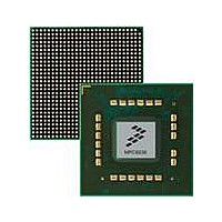
MPC8536DS Freescale Semiconductor, MPC8536DS Datasheet - Page 595

MPC8536DS
Manufacturer Part Number
MPC8536DS
Description
BOARD DEV SYSTEM MPC8536E
Manufacturer
Freescale Semiconductor
Series
PowerQUICC III™r
Type
MPUr
Datasheets
1.MPC8536EBVTAVLA.pdf
(127 pages)
2.MPC8536EBVTAVLA.pdf
(1706 pages)
3.MPC8536DS.pdf
(2 pages)
4.MPC8536DS.pdf
(126 pages)
Specifications of MPC8536DS
Contents
Board, Software and Documentation
Processor Series
MPC85xx
Core
e500
Data Bus Width
32 bit
Maximum Clock Frequency
667 MHz
Operating Supply Voltage
- 0.3 V to + 1.21 V
Maximum Operating Temperature
+ 105 C
Data Ram Size
32 KB
Interface Type
SPI, USB
Program Memory Type
DDR2, DDR3, SDRAM
Core Size
32 Bit
Program Memory Size
544KB
Cpu Speed
1.5GHz
Digital Ic Case Style
BGA
No. Of Pins
783
Supply Voltage Range
0.95V To 1.05V
Rohs Compliant
Yes
For Use With/related Products
MPC8536
Lead Free Status / RoHS Status
Lead free / RoHS Compliant
- MPC8536EBVTAVLA PDF datasheet
- MPC8536EBVTAVLA PDF datasheet #2
- MPC8536DS PDF datasheet #3
- MPC8536DS PDF datasheet #4
- Current page: 595 of 1706
- Download datasheet (15Mb)
Additionally, the following three I
11.2
The following sections give an overview of signals and provide detailed signal descriptions.
11.2.1
The I
signal patterns driven on SDA represent address, data, or read/write information at different stages of the
protocol.
11.2.2
SDA and SCL, described in
devices connected to these two signals must have open-drain or open-collector outputs. The logic AND
function is performed on both of these signals with external pull-up resistors. Refer to the device hardware
specifications for the electrical characteristics of these signals.
Freescale Semiconductor
Signal Name
Serial Clock
(IIC n _SDA)
(IIC n _SCL)
Serial Data
•
•
•
2
C interface uses the SDA and SCL signals, described in
START condition—This condition denotes the beginning of a new data transfer (each data transfer
contains several bytes of data) and awakens all slaves.
Repeated START condition—A START condition that is generated without a STOP condition to
terminate the previous transfer.
STOP condition—The master can terminate the transfer by generating a STOP condition to free
the bus.
External Signal Descriptions
Signal Overview
Detailed Signal Descriptions
Idle State
HIGH
HIGH
MPC8536E PowerQUICC III Integrated Processor Reference Manual, Rev. 1
I/O
O
O
I
I
Table
When the I
to synchronize incoming data on SDA. The bus is assumed to be busy when SCL is detected
low.
As a master, the I
I
When the I
receives data from other
detected low.
When writing as a master or slave, the I
2
C module drives SCL low for data pacing.
Table 11-1. I
2
11-2, serve as a communication interconnect with other devices. All
C-specific states are defined for the I
2
2
C module is idle or acts as a slave, SCL defaults as an input. The unit uses SCL
C module is idle or in a receiving mode, SDA defaults as an input. The unit
2
C Interface Signal Descriptions
2
C module drives SCL along with SDA when transmitting. As a slave, the
I
2
C
devices on SDA. The bus is assumed to be busy when SDA is
State Meaning
2
C module drives data on SDA synchronous to SCL.
Table
11-1, for data transfer. Note that the
2
C interface:
I
2
C Interfaces
11-3
Related parts for MPC8536DS
Image
Part Number
Description
Manufacturer
Datasheet
Request
R
Part Number:
Description:
Manufacturer:
Freescale Semiconductor, Inc
Datasheet:
Part Number:
Description:
Manufacturer:
Freescale Semiconductor, Inc
Datasheet:
Part Number:
Description:
Manufacturer:
Freescale Semiconductor, Inc
Datasheet:
Part Number:
Description:
Manufacturer:
Freescale Semiconductor, Inc
Datasheet:
Part Number:
Description:
Manufacturer:
Freescale Semiconductor, Inc
Datasheet:
Part Number:
Description:
Manufacturer:
Freescale Semiconductor, Inc
Datasheet:
Part Number:
Description:
Manufacturer:
Freescale Semiconductor, Inc
Datasheet:
Part Number:
Description:
Manufacturer:
Freescale Semiconductor, Inc
Datasheet:
Part Number:
Description:
Manufacturer:
Freescale Semiconductor, Inc
Datasheet:
Part Number:
Description:
Manufacturer:
Freescale Semiconductor, Inc
Datasheet:
Part Number:
Description:
Manufacturer:
Freescale Semiconductor, Inc
Datasheet:
Part Number:
Description:
Manufacturer:
Freescale Semiconductor, Inc
Datasheet:
Part Number:
Description:
Manufacturer:
Freescale Semiconductor, Inc
Datasheet:
Part Number:
Description:
Manufacturer:
Freescale Semiconductor, Inc
Datasheet:
Part Number:
Description:
Manufacturer:
Freescale Semiconductor, Inc
Datasheet:


