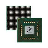
MPC8536DS Freescale Semiconductor, MPC8536DS Datasheet - Page 1670

MPC8536DS
Manufacturer Part Number
MPC8536DS
Description
BOARD DEV SYSTEM MPC8536E
Manufacturer
Freescale Semiconductor
Series
PowerQUICC III™r
Type
MPUr
Datasheets
1.MPC8536EBVTAVLA.pdf
(127 pages)
2.MPC8536EBVTAVLA.pdf
(1706 pages)
3.MPC8536DS.pdf
(2 pages)
4.MPC8536DS.pdf
(126 pages)
Specifications of MPC8536DS
Contents
Board, Software and Documentation
Processor Series
MPC85xx
Core
e500
Data Bus Width
32 bit
Maximum Clock Frequency
667 MHz
Operating Supply Voltage
- 0.3 V to + 1.21 V
Maximum Operating Temperature
+ 105 C
Data Ram Size
32 KB
Interface Type
SPI, USB
Program Memory Type
DDR2, DDR3, SDRAM
Core Size
32 Bit
Program Memory Size
544KB
Cpu Speed
1.5GHz
Digital Ic Case Style
BGA
No. Of Pins
783
Supply Voltage Range
0.95V To 1.05V
Rohs Compliant
Yes
For Use With/related Products
MPC8536
Lead Free Status / RoHS Status
Lead free / RoHS Compliant
- MPC8536EBVTAVLA PDF datasheet
- MPC8536EBVTAVLA PDF datasheet #2
- MPC8536DS PDF datasheet #3
- MPC8536DS PDF datasheet #4
- Current page: 1670 of 1706
- Download datasheet (15Mb)
Revision History
14.7.1.8, 14-234
17.3.10.5, 17-86
17.4.1.8, 17-103
18.1, 18-1
18.3.1.7, 18-12
19.3.3.2, 19-16
20.4.17, 20-36
20.6.5, 20-58
20.6.6, 50-59
21.3.2.11, 21-22
23.4.1.8, 23-14
23.4.1.20, 23-29
23.4.1.28, 23-37
B-6
MPC8536E PowerQUICC III Integrated Processor Reference Manual, Rev. 1
Added the following note:
SGMII mode utilizes the internal TBI PHY. The internal TBI PHY only
auto-negotiates at 1 Gbps. However, 10 Mbps and 100 Mbps speeds are supported
in SGMII mode. It is recommended that the external PHY inform the MAC if the
desired link speed is not 1 Gbps. Software can perform MII management cycles
to determine the external PHY link speed and program ECNTRL and MACCFG2
accordingly.
Changed access of PCI Express Correctable Error Status Register from read/write
to w1c.
Revised first paragraph by deleting “... originating from the PCI Express outbound
ATMUs,” from the first sentence. Also, deleted the last sentence that stated, "Note
that configuration writes originating from the PCI Express configuration access
registers (PEX_CONFIG_ADDR/PEX_CONFIG_DATA) are not serialized."
Changed Figure 19-1, “eSPI Block Diagram,” to show input clock labeled as
“CCB clock divided by 2” rather than “system clock.”
Added note to SPMODEn fields DIV16n and PMn as follows:
“System clock as used here is defined to be CCB clock divided by 2.”
In register SError (SATA Interface Error Register), made bits 10 and 24 Reserved.
For HOSTVER[VVN], added “0x01 Freescale eSDHC version 2.0”
In Table 20-27, “Commands for MMC/SD,” modified Argument column entry for
ACMD23 to read as follows:
[31:23] stuff bits
[22:0] number of blocks”
Modified existing note in section to read as follows:
“When the internal DMA is not enabled and a write transaction is in operation,
DATPORT must not be read. DATPORT also must not be used to read (or write)
data by the CPU or external DMA if the data will be written (or read) by the
eSDHC internal DMA.”
In description of TXFILLTUNING[TXSCHOH], changed formula (introduction
reads “A good value to begin with is:”) as follows:
TXFIFOTHRES (BURSTSIZE 4 bytes-per-word)
(Formerly contained incorrect term BURSTSIZE
Added new register, GENCFGR, “General Configuration Register”
Updated SVR values for silicon revision 1.1 as follows:
0x803F_0091 for MPC8536E Rev 1.1 (with security)
0x8037_0091 for MPC8536 Rev 1.1 (without security).
Feplaced recommended setting for PCI Express in SRDS1CR2[X3SA–X3SF]
(8 bits in all) with “0” (that is, not disabled)
4 bytes-per-word)
(40
Freescale Semiconductor
TimeUnit)
Related parts for MPC8536DS
Image
Part Number
Description
Manufacturer
Datasheet
Request
R
Part Number:
Description:
Manufacturer:
Freescale Semiconductor, Inc
Datasheet:
Part Number:
Description:
Manufacturer:
Freescale Semiconductor, Inc
Datasheet:
Part Number:
Description:
Manufacturer:
Freescale Semiconductor, Inc
Datasheet:
Part Number:
Description:
Manufacturer:
Freescale Semiconductor, Inc
Datasheet:
Part Number:
Description:
Manufacturer:
Freescale Semiconductor, Inc
Datasheet:
Part Number:
Description:
Manufacturer:
Freescale Semiconductor, Inc
Datasheet:
Part Number:
Description:
Manufacturer:
Freescale Semiconductor, Inc
Datasheet:
Part Number:
Description:
Manufacturer:
Freescale Semiconductor, Inc
Datasheet:
Part Number:
Description:
Manufacturer:
Freescale Semiconductor, Inc
Datasheet:
Part Number:
Description:
Manufacturer:
Freescale Semiconductor, Inc
Datasheet:
Part Number:
Description:
Manufacturer:
Freescale Semiconductor, Inc
Datasheet:
Part Number:
Description:
Manufacturer:
Freescale Semiconductor, Inc
Datasheet:
Part Number:
Description:
Manufacturer:
Freescale Semiconductor, Inc
Datasheet:
Part Number:
Description:
Manufacturer:
Freescale Semiconductor, Inc
Datasheet:
Part Number:
Description:
Manufacturer:
Freescale Semiconductor, Inc
Datasheet:


