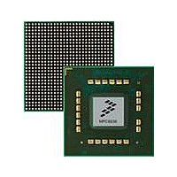
MPC8536DS Freescale Semiconductor, MPC8536DS Datasheet - Page 272

MPC8536DS
Manufacturer Part Number
MPC8536DS
Description
BOARD DEV SYSTEM MPC8536E
Manufacturer
Freescale Semiconductor
Series
PowerQUICC III™r
Type
MPUr
Datasheets
1.MPC8536EBVTAVLA.pdf
(127 pages)
2.MPC8536EBVTAVLA.pdf
(1706 pages)
3.MPC8536DS.pdf
(2 pages)
4.MPC8536DS.pdf
(126 pages)
Specifications of MPC8536DS
Contents
Board, Software and Documentation
Processor Series
MPC85xx
Core
e500
Data Bus Width
32 bit
Maximum Clock Frequency
667 MHz
Operating Supply Voltage
- 0.3 V to + 1.21 V
Maximum Operating Temperature
+ 105 C
Data Ram Size
32 KB
Interface Type
SPI, USB
Program Memory Type
DDR2, DDR3, SDRAM
Core Size
32 Bit
Program Memory Size
544KB
Cpu Speed
1.5GHz
Digital Ic Case Style
BGA
No. Of Pins
783
Supply Voltage Range
0.95V To 1.05V
Rohs Compliant
Yes
For Use With/related Products
MPC8536
Lead Free Status / RoHS Status
Lead free / RoHS Compliant
- MPC8536EBVTAVLA PDF datasheet
- MPC8536EBVTAVLA PDF datasheet #2
- MPC8536DS PDF datasheet #3
- MPC8536DS PDF datasheet #4
- Current page: 272 of 1706
- Download datasheet (15Mb)
e500 Coherency Module
EEBPCR register. Depending how the CPU_RD_HI_DIS field in EEBPCR register is set, read
transactions from the e500 core are initially assigned to either the higher- or lower-bandwidth queue of the
DDR target.
7.3.3
The ECM’s transaction queue performs four basic functions: arbitration across the e500 core and I/O
masters, target mapping and dispatching, enforcement of ordering, and enforcement of coherency. The
address of each transaction is compared against each local access window, and the transaction is then
routed to the appropriate target interface associated with the local access window that the address hits
within. Even though the CCB and ECM allow the pipelining of transactions, the address tenures of all
transactions issued from I/O masters (masters other than the e500 core) may still be ordered. For those
transactions accessing address space marked as snoopable, or space that may be cached by the e500 core,
the ECM enforces coherency, snooping those transactions on the CCB, and taking castouts from the e500
core as is necessary.
7.3.4
Figure 7-1
one 128-bit global data bus. The global data mux allows initiators of write transactions to route data to
their targets and read targets to return data to the initiators.
7.3.5
Figure 7-1
address tenures for the ECM transaction queue. It also contains the queueing and buffering needed to
manage outstanding CCB data tenures. The buffers receive e500 core-initiated write and I/O-initiated read
data (that hit in the L2/SRAM module) from the e500 write (128-bit wide) and read (128-bit wide) data
buses and route them through the global data mux to the global data bus. The buffers also receive e500
core-initiated read and I/O-initiated write data (that hit in the L2/SRAM module) from the global data bus
and forward them onto the CCB data bus (64 bits).
7.4
If the e500 core is used to initialize the device, the CPU boot configuration power-on reset pin should be
pulled high to initially set EEBPCR[CPU_EN]. See
more information on power-up reset initialization.
If any device other than the e500 core (such as PCI Express) is used to initialize the device, the CPU boot
configuration power-on reset pin should be pulled low to initially clear EEBPCR[CPU_EN]. This prevents
the e500 core from accessing any configuration registers or local memory space during initialization.
However, in any such system, one step near the end of the initialization routine must set
EEBPCR[CPU_EN] to re-enable the e500 core. Note that for basic functionality, EEBPCR[CPU_EN] is
the only field that must be written (provided a device other than the e500 core is used to initialize the
device) in the ECM.
7-10
shows how the global data multiplexor takes data bus connections and multiplexes them onto
shows the CCB interface for both CCB address and data tenures. This interface formats CCB
Initialization/Application Information
Transaction Queue
Global Data Multiplexor
CCB Interface
MPC8536E PowerQUICC III Integrated Processor Reference Manual, Rev. 1
Chapter 4, “Reset, Clocking, and
Freescale Semiconductor
Initialization,” for
Related parts for MPC8536DS
Image
Part Number
Description
Manufacturer
Datasheet
Request
R
Part Number:
Description:
Manufacturer:
Freescale Semiconductor, Inc
Datasheet:
Part Number:
Description:
Manufacturer:
Freescale Semiconductor, Inc
Datasheet:
Part Number:
Description:
Manufacturer:
Freescale Semiconductor, Inc
Datasheet:
Part Number:
Description:
Manufacturer:
Freescale Semiconductor, Inc
Datasheet:
Part Number:
Description:
Manufacturer:
Freescale Semiconductor, Inc
Datasheet:
Part Number:
Description:
Manufacturer:
Freescale Semiconductor, Inc
Datasheet:
Part Number:
Description:
Manufacturer:
Freescale Semiconductor, Inc
Datasheet:
Part Number:
Description:
Manufacturer:
Freescale Semiconductor, Inc
Datasheet:
Part Number:
Description:
Manufacturer:
Freescale Semiconductor, Inc
Datasheet:
Part Number:
Description:
Manufacturer:
Freescale Semiconductor, Inc
Datasheet:
Part Number:
Description:
Manufacturer:
Freescale Semiconductor, Inc
Datasheet:
Part Number:
Description:
Manufacturer:
Freescale Semiconductor, Inc
Datasheet:
Part Number:
Description:
Manufacturer:
Freescale Semiconductor, Inc
Datasheet:
Part Number:
Description:
Manufacturer:
Freescale Semiconductor, Inc
Datasheet:
Part Number:
Description:
Manufacturer:
Freescale Semiconductor, Inc
Datasheet:


