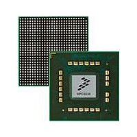
MPC8536DS Freescale Semiconductor, MPC8536DS Datasheet - Page 683

MPC8536DS
Manufacturer Part Number
MPC8536DS
Description
BOARD DEV SYSTEM MPC8536E
Manufacturer
Freescale Semiconductor
Series
PowerQUICC III™r
Type
MPUr
Datasheets
1.MPC8536EBVTAVLA.pdf
(127 pages)
2.MPC8536EBVTAVLA.pdf
(1706 pages)
3.MPC8536DS.pdf
(2 pages)
4.MPC8536DS.pdf
(126 pages)
Specifications of MPC8536DS
Contents
Board, Software and Documentation
Processor Series
MPC85xx
Core
e500
Data Bus Width
32 bit
Maximum Clock Frequency
667 MHz
Operating Supply Voltage
- 0.3 V to + 1.21 V
Maximum Operating Temperature
+ 105 C
Data Ram Size
32 KB
Interface Type
SPI, USB
Program Memory Type
DDR2, DDR3, SDRAM
Core Size
32 Bit
Program Memory Size
544KB
Cpu Speed
1.5GHz
Digital Ic Case Style
BGA
No. Of Pins
783
Supply Voltage Range
0.95V To 1.05V
Rohs Compliant
Yes
For Use With/related Products
MPC8536
Lead Free Status / RoHS Status
Lead free / RoHS Compliant
- MPC8536EBVTAVLA PDF datasheet
- MPC8536EBVTAVLA PDF datasheet #2
- MPC8536DS PDF datasheet #3
- MPC8536DS PDF datasheet #4
- Current page: 683 of 1706
- Download datasheet (15Mb)
13.3.1.22 Flash Byte Count Register (FBCR)
The local bus Flash byte count register (FBCR), shown in
transfers for reads and writes to the NAND Flash EEPROM.
Table 13-30
13.3.1.23 Flash ECC Block n Register (FECC0–FECC3)
The local bus flash ECC blockn register (FECCn), shown in
calculated during writes or reads by eLBC. It can be used for verify after write feature in software. Note
that the valid bit sets before the command completion event and hence the correct ECC could be read
before actual completion of writes/reads.
Freescale Semiconductor
Offset 0x0_50F4
Offset FECC0: 0x0_5100
Reset
20–31
0–19
Bits
W
W
R
R V
FECC1: 0x0_5104
FECC2: 0x0_5108
FECC3: 0x0_510C
0
0
Name
1
BC
describes FBCR fields.
—
Reserved
Byte count determines how many bytes are transferred by the FCM during data read (RB) or data write
(WB) opcodes.
The first byte accessed in the NAND Flash EEPROM is located by the FPAR register, and successive
bytes are transferred until either BC bytes have been counted, or the end of the spare region of the
currently addressed Flash page has been reached.
If BC = 0, an entire Flash page and its spare region will be transferred by FCM, in which case
FPAR[MS] and FPAR[CI] are treated as zero regardless of their values. BC = 0 is the only setting that
permits FCM to generate and check ECC.
MPC8536E PowerQUICC III Integrated Processor Reference Manual, Rev. 1
—
Figure 13-28. Flash ECC Block n Register (FECC0–FECC3)
7
—
8
Figure 13-27. Flash Byte Count Register
Table 13-30. FBCR Field Descriptions
All zeros
19 20
Description
Figure
Figure
13-27, defines the size of FCM block
ECC
13-28, specifies the ECC value
BC
Enhanced Local Bus Controller
Access: Read/Write
Access: Read Only
13-41
31
31
Related parts for MPC8536DS
Image
Part Number
Description
Manufacturer
Datasheet
Request
R
Part Number:
Description:
Manufacturer:
Freescale Semiconductor, Inc
Datasheet:
Part Number:
Description:
Manufacturer:
Freescale Semiconductor, Inc
Datasheet:
Part Number:
Description:
Manufacturer:
Freescale Semiconductor, Inc
Datasheet:
Part Number:
Description:
Manufacturer:
Freescale Semiconductor, Inc
Datasheet:
Part Number:
Description:
Manufacturer:
Freescale Semiconductor, Inc
Datasheet:
Part Number:
Description:
Manufacturer:
Freescale Semiconductor, Inc
Datasheet:
Part Number:
Description:
Manufacturer:
Freescale Semiconductor, Inc
Datasheet:
Part Number:
Description:
Manufacturer:
Freescale Semiconductor, Inc
Datasheet:
Part Number:
Description:
Manufacturer:
Freescale Semiconductor, Inc
Datasheet:
Part Number:
Description:
Manufacturer:
Freescale Semiconductor, Inc
Datasheet:
Part Number:
Description:
Manufacturer:
Freescale Semiconductor, Inc
Datasheet:
Part Number:
Description:
Manufacturer:
Freescale Semiconductor, Inc
Datasheet:
Part Number:
Description:
Manufacturer:
Freescale Semiconductor, Inc
Datasheet:
Part Number:
Description:
Manufacturer:
Freescale Semiconductor, Inc
Datasheet:
Part Number:
Description:
Manufacturer:
Freescale Semiconductor, Inc
Datasheet:


