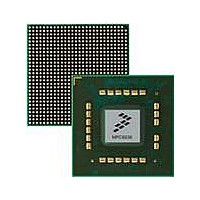
MPC8536DS Freescale Semiconductor, MPC8536DS Datasheet - Page 550

MPC8536DS
Manufacturer Part Number
MPC8536DS
Description
BOARD DEV SYSTEM MPC8536E
Manufacturer
Freescale Semiconductor
Series
PowerQUICC III™r
Type
MPUr
Datasheets
1.MPC8536EBVTAVLA.pdf
(127 pages)
2.MPC8536EBVTAVLA.pdf
(1706 pages)
3.MPC8536DS.pdf
(2 pages)
4.MPC8536DS.pdf
(126 pages)
Specifications of MPC8536DS
Contents
Board, Software and Documentation
Processor Series
MPC85xx
Core
e500
Data Bus Width
32 bit
Maximum Clock Frequency
667 MHz
Operating Supply Voltage
- 0.3 V to + 1.21 V
Maximum Operating Temperature
+ 105 C
Data Ram Size
32 KB
Interface Type
SPI, USB
Program Memory Type
DDR2, DDR3, SDRAM
Core Size
32 Bit
Program Memory Size
544KB
Cpu Speed
1.5GHz
Digital Ic Case Style
BGA
No. Of Pins
783
Supply Voltage Range
0.95V To 1.05V
Rohs Compliant
Yes
For Use With/related Products
MPC8536
Lead Free Status / RoHS Status
Lead free / RoHS Compliant
- MPC8536EBVTAVLA PDF datasheet
- MPC8536EBVTAVLA PDF datasheet #2
- MPC8536DS PDF datasheet #3
- MPC8536DS PDF datasheet #4
- Current page: 550 of 1706
- Download datasheet (15Mb)
Security Engine (SEC) 3.0
10.7.5.3
The KEU data size register (shown in
message word. As Kasumi allows for bit level granularity for encryption/decryption, there are no illegal
data sizes. The proper bit length of the message must be written to notify the KEU of any padding
performed by the host. This register is cleared when the KEU is reset or re-initialized.
Writing to this register signals the KEU to start processing data from the input FIFO as soon as it is
available. If the value of data size is modified during processing, a context error is generated.
Kasumi processing is determined by both the data size and the setting of the process end of message (PE)
bit in the KEU mode register. The PE bit determines how the final block of message data is processed. In
typical descriptor-based operations, the data size register is loaded with values which are an integral
number of bytes. For descriptor based f8 operations, the software is responsible for padding the data to the
next byte boundary, and for removing this padding from the KEU’s output. The output of the KEU is an
integral number of bytes, as specified in the descriptor, automatically truncating any internal padding
required to process the final 64 bits message block. As the KEU can infer when it has reached the final
64 bits message block from the length fields in the descriptor, setting the PE bit through the descriptor
header is not required. While performing f8 operations, the KEU’s output is the same irrespective of the
setting of the PE bit.
For the descriptor-based f9 operations, the PE bit must be set through the descriptor header whenever the
descriptor is being used to process the final message block. This causes the KEU to automatically pad the
final block before calculating the f9 MAC.
The details of data size register and the PE interaction are more relevant when operating the KEU in direct
access (slave) mode, rather than using descriptors. Note that operating the KEU in direct access mode is
not recommended other than for debug test cases, and the information provided here regarding the use of
data size and PE in direct access mode is to explain the behaviors that might be encountered in direct access
debug operations.
PE has the following effects for direct access mode f8 operations, using the example of a 64-bit f8
keystream ‘0x1234567890abcdef’ and the data size register containing ‘0x0a’ (10 bits = 1 byte + 2 bits):
10-120
Offset 0xE010
Reset
•
•
W
R
0
PE = 0: The final ten message bits are XORed with the entire last 64-bit block of keystream, which
produces 54 additional non-zero bits after the end of the real message. These additional 54 bits
must be removed by the software.
PE = 1: The final ten message bits are XORed with ten bits of keystream ’0x120’, and no additional
bits of the false message are produced.
KEU Data Size Register (KEUDSR)
MPC8536E PowerQUICC III Integrated Processor Reference Manual, Rev. 1
Figure 10-66. KEU Data Size Register
Figure
—
10-66) stores the number of bits to process in the final
All zeros
51 52
Data Size (bits)
Freescale Semiconductor
Access: Read/Write
63
Related parts for MPC8536DS
Image
Part Number
Description
Manufacturer
Datasheet
Request
R
Part Number:
Description:
Manufacturer:
Freescale Semiconductor, Inc
Datasheet:
Part Number:
Description:
Manufacturer:
Freescale Semiconductor, Inc
Datasheet:
Part Number:
Description:
Manufacturer:
Freescale Semiconductor, Inc
Datasheet:
Part Number:
Description:
Manufacturer:
Freescale Semiconductor, Inc
Datasheet:
Part Number:
Description:
Manufacturer:
Freescale Semiconductor, Inc
Datasheet:
Part Number:
Description:
Manufacturer:
Freescale Semiconductor, Inc
Datasheet:
Part Number:
Description:
Manufacturer:
Freescale Semiconductor, Inc
Datasheet:
Part Number:
Description:
Manufacturer:
Freescale Semiconductor, Inc
Datasheet:
Part Number:
Description:
Manufacturer:
Freescale Semiconductor, Inc
Datasheet:
Part Number:
Description:
Manufacturer:
Freescale Semiconductor, Inc
Datasheet:
Part Number:
Description:
Manufacturer:
Freescale Semiconductor, Inc
Datasheet:
Part Number:
Description:
Manufacturer:
Freescale Semiconductor, Inc
Datasheet:
Part Number:
Description:
Manufacturer:
Freescale Semiconductor, Inc
Datasheet:
Part Number:
Description:
Manufacturer:
Freescale Semiconductor, Inc
Datasheet:
Part Number:
Description:
Manufacturer:
Freescale Semiconductor, Inc
Datasheet:


