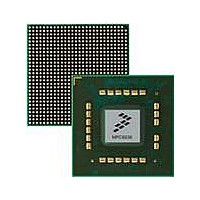
MPC8536DS Freescale Semiconductor, MPC8536DS Datasheet - Page 144

MPC8536DS
Manufacturer Part Number
MPC8536DS
Description
BOARD DEV SYSTEM MPC8536E
Manufacturer
Freescale Semiconductor
Series
PowerQUICC III™r
Type
MPUr
Datasheets
1.MPC8536EBVTAVLA.pdf
(127 pages)
2.MPC8536EBVTAVLA.pdf
(1706 pages)
3.MPC8536DS.pdf
(2 pages)
4.MPC8536DS.pdf
(126 pages)
Specifications of MPC8536DS
Contents
Board, Software and Documentation
Processor Series
MPC85xx
Core
e500
Data Bus Width
32 bit
Maximum Clock Frequency
667 MHz
Operating Supply Voltage
- 0.3 V to + 1.21 V
Maximum Operating Temperature
+ 105 C
Data Ram Size
32 KB
Interface Type
SPI, USB
Program Memory Type
DDR2, DDR3, SDRAM
Core Size
32 Bit
Program Memory Size
544KB
Cpu Speed
1.5GHz
Digital Ic Case Style
BGA
No. Of Pins
783
Supply Voltage Range
0.95V To 1.05V
Rohs Compliant
Yes
For Use With/related Products
MPC8536
Lead Free Status / RoHS Status
Lead free / RoHS Compliant
- MPC8536EBVTAVLA PDF datasheet
- MPC8536EBVTAVLA PDF datasheet #2
- MPC8536DS PDF datasheet #3
- MPC8536DS PDF datasheet #4
- Current page: 144 of 1706
- Download datasheet (15Mb)
Memory Map
address space can be supported.See
detailed description of the PCI Express outbound ATMU windows.
2.2.5
Inbound address translation and mapping refers to the translation of an address from the external address
space of an I/O interface (such as PCI address space) to the local 36-bit address space understood by the
internal interfaces of the MPC8536. It also refers to the mapping of transactions to a particular target
interface and the assignment of transaction attributes. The PCI and the PCI Express controllers have
inbound address translation and mapping units (ATMUs).
2.2.5.1
The PCI controller has three general inbound ATMU windows plus a dedicated window for memory
mapped configuration accesses (PCSRBAR). These windows have a one-to-one correspondence with the
base address registers in the PCI programming model. Updating one automatically updates the other. There
is no default inbound window; if a PCI address does not match one of the inbound ATMU windows, the
device does not respond with an assertion of PCI_DEVSEL. See
Registers,”
2.2.5.2
The PCI Express controller has three inbound ATMU windows plus a default. See
Express Outbound ATMU Registers,”
2.2.5.3
Since both local access windows and inbound ATMUs map transactions to a target interface, it is essential
that they not contradict one another. For instance, it is a programming error to have an inbound ATMU map
a transaction to the DDR SDRAM memory controller (target interface 0b1111) if the resulting translated local
address is mapped to PCI (target interface 0b0000) by a local access window. Such a programming error may
result in unpredictable system deadlocks.
2.3
All of the memory mapped configuration, control, and status registers in the MPC8536 are contained
within a 1-Mbyte address region. To allow for flexibility, the configuration, control, and status block is
relocatable in the local address space. The local address map location of this register block is controlled
by the configuration, control, and status registers base address register (CCSRBAR), see
“Configuration, Control, and Status Registers Base Address Register (CCSRBAR).”
CCSRBAR is 4 Gbytes–9 Mbytes, or 0x0_FF70_0000.
2-10
Configuration, Control, and Status Register Map
for a detailed description of the PCI inbound ATMU windows.
Inbound Address Translation and Mapping Windows
PCI Inbound ATMU
PCI Express Inbound ATMU
Illegal Interaction Between Inbound ATMUs and Local Access Windows
The configuration, control, and status window must not overlap a local
access window that maps to the DDR controller. Otherwise, undefined
behavior occurs.
MPC8536E PowerQUICC III Integrated Processor Reference Manual, Rev. 1
Section 17.3.5.1, “PCI Express Outbound ATMU Registers”
for a description of the PCI Express inbound ATMU windows.
NOTE
Section 16.3.1.3, “PCI ATMU Inbound
Section 17.3.5.1, “PCI
The default value for
Freescale Semiconductor
Section 4.3.1.1.2,
for a
Related parts for MPC8536DS
Image
Part Number
Description
Manufacturer
Datasheet
Request
R
Part Number:
Description:
Manufacturer:
Freescale Semiconductor, Inc
Datasheet:
Part Number:
Description:
Manufacturer:
Freescale Semiconductor, Inc
Datasheet:
Part Number:
Description:
Manufacturer:
Freescale Semiconductor, Inc
Datasheet:
Part Number:
Description:
Manufacturer:
Freescale Semiconductor, Inc
Datasheet:
Part Number:
Description:
Manufacturer:
Freescale Semiconductor, Inc
Datasheet:
Part Number:
Description:
Manufacturer:
Freescale Semiconductor, Inc
Datasheet:
Part Number:
Description:
Manufacturer:
Freescale Semiconductor, Inc
Datasheet:
Part Number:
Description:
Manufacturer:
Freescale Semiconductor, Inc
Datasheet:
Part Number:
Description:
Manufacturer:
Freescale Semiconductor, Inc
Datasheet:
Part Number:
Description:
Manufacturer:
Freescale Semiconductor, Inc
Datasheet:
Part Number:
Description:
Manufacturer:
Freescale Semiconductor, Inc
Datasheet:
Part Number:
Description:
Manufacturer:
Freescale Semiconductor, Inc
Datasheet:
Part Number:
Description:
Manufacturer:
Freescale Semiconductor, Inc
Datasheet:
Part Number:
Description:
Manufacturer:
Freescale Semiconductor, Inc
Datasheet:
Part Number:
Description:
Manufacturer:
Freescale Semiconductor, Inc
Datasheet:


