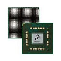
MPC8536DS Freescale Semiconductor, MPC8536DS Datasheet - Page 724

MPC8536DS
Manufacturer Part Number
MPC8536DS
Description
BOARD DEV SYSTEM MPC8536E
Manufacturer
Freescale Semiconductor
Series
PowerQUICC III™r
Type
MPUr
Datasheets
1.MPC8536EBVTAVLA.pdf
(127 pages)
2.MPC8536EBVTAVLA.pdf
(1706 pages)
3.MPC8536DS.pdf
(2 pages)
4.MPC8536DS.pdf
(126 pages)
Specifications of MPC8536DS
Contents
Board, Software and Documentation
Processor Series
MPC85xx
Core
e500
Data Bus Width
32 bit
Maximum Clock Frequency
667 MHz
Operating Supply Voltage
- 0.3 V to + 1.21 V
Maximum Operating Temperature
+ 105 C
Data Ram Size
32 KB
Interface Type
SPI, USB
Program Memory Type
DDR2, DDR3, SDRAM
Core Size
32 Bit
Program Memory Size
544KB
Cpu Speed
1.5GHz
Digital Ic Case Style
BGA
No. Of Pins
783
Supply Voltage Range
0.95V To 1.05V
Rohs Compliant
Yes
For Use With/related Products
MPC8536
Lead Free Status / RoHS Status
Lead free / RoHS Compliant
- MPC8536EBVTAVLA PDF datasheet
- MPC8536EBVTAVLA PDF datasheet #2
- MPC8536DS PDF datasheet #3
- MPC8536DS PDF datasheet #4
- Current page: 724 of 1706
- Download datasheet (15Mb)
Enhanced Local Bus Controller
13-82
22–23
Bits
16
17
18
19
20
21
24
G4T3/WAEN General purpose line 4 timing 3/wait enable. Bit function is determined by M x MR[GPL4].
G4T1/DLT3 General purpose line 4 timing 1/delay time 3. The function of this bit is determined by
REDO
Name
LOOP
G3T1
G3T3
G5T1
G5T3
MPC8536E PowerQUICC III Integrated Processor Reference Manual, Rev. 1
phases 1 and 2 (first half phase).
phases 3 and 4 (second half phase).
M x MR[GPL4].
If M x MR[GPL4] = 0 and LGPL4/LUPWAIT pin functions as an output (LGPL4), G4T1/DLT3
defines the state (0 or 1) of LGPL4 during bus clock quarter phases 1 and 2 (first half phase).
If M x MR[GPL4] = 1 and LGPL4/LUPWAIT functions as an input (LUPWAIT), if a read burst or
single read is executed, G4T1/DLT3 defines the sampling of the data bus as follows:
0 In the current word, the data bus should be sampled at the start of bus clock quarter phase
1 In the current word, the data bus should be sampled at the start of bus clock quarter phase
If M x MR[GPL4] = 0 and LGPL4/LUPWAIT pin functions as an output (LGPL4), G4T3/WAEN
defines the state (0 or 1) of LGPL4 during bus clock quarter phases 3 and 4 (second half phase).
If M x MR[GPL4] = 1 and LGPL4/LUPWAIT functions as an input (LUPWAIT), G4T3/WAEN is
used to enable the wait mechanism:
0 LUPWAIT detection is disabled.
1 LUPWAIT is enabled. If LUPWAIT is detected as being asserted, a freeze in the external
phases 1 and 2 (first half phase).
phases 3 and 4 (second half phase).
00 Once (normal operation)
01 Twice
10 Three times
11 Four times
Loop start/end. The first RAM word in the RAM array where LOOP is 1 is recognized as the loop
start word. The next RAM word where LOOP is 1 is the loop end word. RAM words between,
and including the start and end words, are defined as part of the loop. The number of times the
UPM executes this loop is defined in the corresponding loop fields of the M x MR.
0 The current RAM word is not the loop start word or loop end word.
1 The current RAM word is the start or end of a loop.
Note: AMX must not change values in any RAM word which begins a loop
General purpose line 3 timing 1. Defines the state (0 or 1) of LGPL3 during bus clock quarter
General purpose line 3 timing 3. Defines the state (0 or 1) of LGPL3 during bus clock quarter
General purpose line 5 timing 1. Defines the state (0 or 1) of LGPL5 during bus clock quarter
General purpose line 5 timing 3. Defines the state (0 or 1) of LGPL5 during bus clock quarter
Redo current RAM word. Defines the number of times to execute the current RAM word.
1 of the next bus clock cycle.
3 of the current bus clock cycle.
signals logical values occurs until LUPWAIT is detected as being negated.
Table 13-40. RAM Word Field Descriptions (continued)
Description
Freescale Semiconductor
Related parts for MPC8536DS
Image
Part Number
Description
Manufacturer
Datasheet
Request
R
Part Number:
Description:
Manufacturer:
Freescale Semiconductor, Inc
Datasheet:
Part Number:
Description:
Manufacturer:
Freescale Semiconductor, Inc
Datasheet:
Part Number:
Description:
Manufacturer:
Freescale Semiconductor, Inc
Datasheet:
Part Number:
Description:
Manufacturer:
Freescale Semiconductor, Inc
Datasheet:
Part Number:
Description:
Manufacturer:
Freescale Semiconductor, Inc
Datasheet:
Part Number:
Description:
Manufacturer:
Freescale Semiconductor, Inc
Datasheet:
Part Number:
Description:
Manufacturer:
Freescale Semiconductor, Inc
Datasheet:
Part Number:
Description:
Manufacturer:
Freescale Semiconductor, Inc
Datasheet:
Part Number:
Description:
Manufacturer:
Freescale Semiconductor, Inc
Datasheet:
Part Number:
Description:
Manufacturer:
Freescale Semiconductor, Inc
Datasheet:
Part Number:
Description:
Manufacturer:
Freescale Semiconductor, Inc
Datasheet:
Part Number:
Description:
Manufacturer:
Freescale Semiconductor, Inc
Datasheet:
Part Number:
Description:
Manufacturer:
Freescale Semiconductor, Inc
Datasheet:
Part Number:
Description:
Manufacturer:
Freescale Semiconductor, Inc
Datasheet:
Part Number:
Description:
Manufacturer:
Freescale Semiconductor, Inc
Datasheet:


