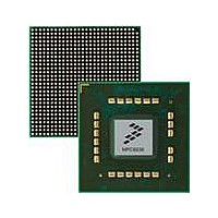
MPC8536DS Freescale Semiconductor, MPC8536DS Datasheet - Page 348

MPC8536DS
Manufacturer Part Number
MPC8536DS
Description
BOARD DEV SYSTEM MPC8536E
Manufacturer
Freescale Semiconductor
Series
PowerQUICC III™r
Type
MPUr
Datasheets
1.MPC8536EBVTAVLA.pdf
(127 pages)
2.MPC8536EBVTAVLA.pdf
(1706 pages)
3.MPC8536DS.pdf
(2 pages)
4.MPC8536DS.pdf
(126 pages)
Specifications of MPC8536DS
Contents
Board, Software and Documentation
Processor Series
MPC85xx
Core
e500
Data Bus Width
32 bit
Maximum Clock Frequency
667 MHz
Operating Supply Voltage
- 0.3 V to + 1.21 V
Maximum Operating Temperature
+ 105 C
Data Ram Size
32 KB
Interface Type
SPI, USB
Program Memory Type
DDR2, DDR3, SDRAM
Core Size
32 Bit
Program Memory Size
544KB
Cpu Speed
1.5GHz
Digital Ic Case Style
BGA
No. Of Pins
783
Supply Voltage Range
0.95V To 1.05V
Rohs Compliant
Yes
For Use With/related Products
MPC8536
Lead Free Status / RoHS Status
Lead free / RoHS Compliant
- MPC8536EBVTAVLA PDF datasheet
- MPC8536EBVTAVLA PDF datasheet #2
- MPC8536DS PDF datasheet #3
- MPC8536DS PDF datasheet #4
- Current page: 348 of 1706
- Download datasheet (15Mb)
DDR Memory Controller
The value of the above parameters (in whole clock cycles) must be set by boot code at system start-up (in
the TIMING_CFG_0, TIMING_CFG_1, TIMING_CFG_2, and TIMING_CFG_3 registers as described
in
SDRAM Timing Configuration 1 (TIMING_CFG_1),” Section 8.4.1.7, “DDR SDRAM Timing
Configuration 2 (TIMING_CFG_2),”
(TIMING_CFG_3)”) and be kept in the DDR memory controller configuration register space.
The following figures show SDRAM timing for various types of accesses. System software is responsible
(at reset) for optimally configuring SDRAM timing parameters. The programmable timing parameters
apply to both read and write timing configuration. The configuration process must be completed and the
DDR SDRAM initialized before any accesses to SDRAM are attempted.
Figure 8-49
for a single-beat read operation,
word write operation. Note that all signal transitions occur on the rising edge of the memory bus clock and
that single-beat read operations are identical to burst-reads. These figures assume the CLK_ADJUST is
set to 1/2 DRAM cycle, an additive latency of 0 DRAM cycles is used, and the write latency is 1 DRAM
cycle.
8-74
Section 8.4.1.5, “DDR SDRAM Timing Configuration 0 (TIMING_CFG_0),” Section 8.4.1.6, “DDR
SDRAM Clock
through
Figure 8-49. DDR SDRAM Burst Read Timing—ACTTORW = 3, MCAS Latency = 2
MDQS
MRAS
MCAS
MDQ n
MWE
MCS
MA n
MPC8536E PowerQUICC III Integrated Processor Reference Manual, Rev. 1
Figure 8-51
ROW
0
Figure 8-50
1
show DDR SDRAM timing for various types of accesses; see
ACTTORW
2
and
COL
Section 8.4.1.4, “DDR SDRAM Timing Configuration 3
3
for a single-beat write operation, and
CASLAT
4
COL
5
D0
D1 D2 D3
6
7
D0
D1 D2
8
D3
9
10
Figure 8-51
Freescale Semiconductor
11
12
for a double
Figure 8-49
Related parts for MPC8536DS
Image
Part Number
Description
Manufacturer
Datasheet
Request
R
Part Number:
Description:
Manufacturer:
Freescale Semiconductor, Inc
Datasheet:
Part Number:
Description:
Manufacturer:
Freescale Semiconductor, Inc
Datasheet:
Part Number:
Description:
Manufacturer:
Freescale Semiconductor, Inc
Datasheet:
Part Number:
Description:
Manufacturer:
Freescale Semiconductor, Inc
Datasheet:
Part Number:
Description:
Manufacturer:
Freescale Semiconductor, Inc
Datasheet:
Part Number:
Description:
Manufacturer:
Freescale Semiconductor, Inc
Datasheet:
Part Number:
Description:
Manufacturer:
Freescale Semiconductor, Inc
Datasheet:
Part Number:
Description:
Manufacturer:
Freescale Semiconductor, Inc
Datasheet:
Part Number:
Description:
Manufacturer:
Freescale Semiconductor, Inc
Datasheet:
Part Number:
Description:
Manufacturer:
Freescale Semiconductor, Inc
Datasheet:
Part Number:
Description:
Manufacturer:
Freescale Semiconductor, Inc
Datasheet:
Part Number:
Description:
Manufacturer:
Freescale Semiconductor, Inc
Datasheet:
Part Number:
Description:
Manufacturer:
Freescale Semiconductor, Inc
Datasheet:
Part Number:
Description:
Manufacturer:
Freescale Semiconductor, Inc
Datasheet:
Part Number:
Description:
Manufacturer:
Freescale Semiconductor, Inc
Datasheet:


