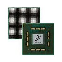
MPC8536DS Freescale Semiconductor, MPC8536DS Datasheet - Page 1037

MPC8536DS
Manufacturer Part Number
MPC8536DS
Description
BOARD DEV SYSTEM MPC8536E
Manufacturer
Freescale Semiconductor
Series
PowerQUICC III™r
Type
MPUr
Datasheets
1.MPC8536EBVTAVLA.pdf
(127 pages)
2.MPC8536EBVTAVLA.pdf
(1706 pages)
3.MPC8536DS.pdf
(2 pages)
4.MPC8536DS.pdf
(126 pages)
Specifications of MPC8536DS
Contents
Board, Software and Documentation
Processor Series
MPC85xx
Core
e500
Data Bus Width
32 bit
Maximum Clock Frequency
667 MHz
Operating Supply Voltage
- 0.3 V to + 1.21 V
Maximum Operating Temperature
+ 105 C
Data Ram Size
32 KB
Interface Type
SPI, USB
Program Memory Type
DDR2, DDR3, SDRAM
Core Size
32 Bit
Program Memory Size
544KB
Cpu Speed
1.5GHz
Digital Ic Case Style
BGA
No. Of Pins
783
Supply Voltage Range
0.95V To 1.05V
Rohs Compliant
Yes
For Use With/related Products
MPC8536
Lead Free Status / RoHS Status
Lead free / RoHS Compliant
- MPC8536EBVTAVLA PDF datasheet
- MPC8536EBVTAVLA PDF datasheet #2
- MPC8536DS PDF datasheet #3
- MPC8536DS PDF datasheet #4
- Current page: 1037 of 1706
- Download datasheet (15Mb)
16.3
The PCI controller supports the following two types of registers:
16.3.1
The PCI memory mapped registers are accessed by reading and writing to an address comprised of the base
address (specified in the CCSRBAR on the local side or the PCSRBAR on the PCI side) plus the block
base address, plus the offset of the specific register to be accessed. Note that all memory-mapped registers
(except the PCI configuration data register, PCI CFG_DATA) must only be accessed as 32-bit quantities.
Table 16-3
Freescale Semiconductor
0x00C–
0xBFC
Offset
0xC00
0xC04
0x000
0x004
0x008
•
•
PCI_CLK
Signal
Memory-mapped registers—these registers control PCI address translation, PCI error
management, and PCI configuration register access. These registers are described in
Section 16.3.1, “PCI Memory-Mapped Registers,”
PCI configuration registers contained within the PCI configuration header—these registers are
specified by the PCI bus specification for every PCI device. These registers are described in
Section 16.3.2, “PCI Configuration Header,”
Memory Map/Register Definitions
CFG_ADDR—PCI configuration address
CFG_DATA—PCI configuration data
INT_ACK—PCI interrupt acknowledge
Reserved
POTAR0—PCI outbound window 0 (default) translation address
register
POTEAR0—PCI outbound window 0 (default) translation extended
address register
lists the memory-mapped registers.
PCI Memory-Mapped Registers
Table 16-2. PCI Interface Signals—Detailed Signal Descriptions (continued)
I/O
I PCI clock is an independent clock that may be used for the PCI interface. If used the PCI operation is
PCI Controller Memory-Mapped Registers—Block Base Address 0x0_8000
MPC8536E PowerQUICC III Integrated Processor Reference Manual, Rev. 1
asynchronous with respect to SYSCLK and the platform clock. In order to used this signal as the PCI
clock source, it must be designated during POR configuration. See the reset chapter for POR details
regarding clock selection as well as proper PCI frequency selection.
Timing Assertion/Negation—See the device Hardware Specification for specific timing information.
Table 16-3. PCI Memory-Mapped Register Map
PCI ATMU Registers—Outbound and Inbound
0xC00–0xC3C–Outbound Window 0 (default)
Register
PCI Configuration Access Registers
and its subsections.
Description
and its subsections.
Access
R/W
R/W
R/W
R/W
—
R
0x0000_0000
0x0000_0000
0x0000_0000
0x0000_0000
0x0000_0000
Reset
—
16.3.1.1.1/16-14
16.3.1.1.2/16-15
16.3.1.1.3/16-15
16.3.1.2.1/16-16
16.3.1.2.2/16-16
PCI Bus Interface
Section/page
—
16-11
Related parts for MPC8536DS
Image
Part Number
Description
Manufacturer
Datasheet
Request
R
Part Number:
Description:
Manufacturer:
Freescale Semiconductor, Inc
Datasheet:
Part Number:
Description:
Manufacturer:
Freescale Semiconductor, Inc
Datasheet:
Part Number:
Description:
Manufacturer:
Freescale Semiconductor, Inc
Datasheet:
Part Number:
Description:
Manufacturer:
Freescale Semiconductor, Inc
Datasheet:
Part Number:
Description:
Manufacturer:
Freescale Semiconductor, Inc
Datasheet:
Part Number:
Description:
Manufacturer:
Freescale Semiconductor, Inc
Datasheet:
Part Number:
Description:
Manufacturer:
Freescale Semiconductor, Inc
Datasheet:
Part Number:
Description:
Manufacturer:
Freescale Semiconductor, Inc
Datasheet:
Part Number:
Description:
Manufacturer:
Freescale Semiconductor, Inc
Datasheet:
Part Number:
Description:
Manufacturer:
Freescale Semiconductor, Inc
Datasheet:
Part Number:
Description:
Manufacturer:
Freescale Semiconductor, Inc
Datasheet:
Part Number:
Description:
Manufacturer:
Freescale Semiconductor, Inc
Datasheet:
Part Number:
Description:
Manufacturer:
Freescale Semiconductor, Inc
Datasheet:
Part Number:
Description:
Manufacturer:
Freescale Semiconductor, Inc
Datasheet:
Part Number:
Description:
Manufacturer:
Freescale Semiconductor, Inc
Datasheet:


