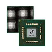
MPC8536DS Freescale Semiconductor, MPC8536DS Datasheet - Page 225

MPC8536DS
Manufacturer Part Number
MPC8536DS
Description
BOARD DEV SYSTEM MPC8536E
Manufacturer
Freescale Semiconductor
Series
PowerQUICC III™r
Type
MPUr
Datasheets
1.MPC8536EBVTAVLA.pdf
(127 pages)
2.MPC8536EBVTAVLA.pdf
(1706 pages)
3.MPC8536DS.pdf
(2 pages)
4.MPC8536DS.pdf
(126 pages)
Specifications of MPC8536DS
Contents
Board, Software and Documentation
Processor Series
MPC85xx
Core
e500
Data Bus Width
32 bit
Maximum Clock Frequency
667 MHz
Operating Supply Voltage
- 0.3 V to + 1.21 V
Maximum Operating Temperature
+ 105 C
Data Ram Size
32 KB
Interface Type
SPI, USB
Program Memory Type
DDR2, DDR3, SDRAM
Core Size
32 Bit
Program Memory Size
544KB
Cpu Speed
1.5GHz
Digital Ic Case Style
BGA
No. Of Pins
783
Supply Voltage Range
0.95V To 1.05V
Rohs Compliant
Yes
For Use With/related Products
MPC8536
Lead Free Status / RoHS Status
Lead free / RoHS Compliant
- MPC8536EBVTAVLA PDF datasheet
- MPC8536EBVTAVLA PDF datasheet #2
- MPC8536DS PDF datasheet #3
- MPC8536DS PDF datasheet #4
- Current page: 225 of 1706
- Download datasheet (15Mb)
6.2.1
Figure 6-3
Physical address bits 20–30 identify the bank and set of the tag and data. Physical address bits 0–19 are
compared against the tags of all eight ways. A match of a valid tag selects a 32-byte block of data (or way)
within the set. Physical address bits 31–35 identify the byte or bytes of data within the block.
6.2.2
When all or part of the array is dedicated to memory mapped SRAM, individual ways of each set are
reserved for that purpose. SRAM accesses use physical address bits 17–19 in conjunction with the SRAM
mode to select a way of the indexed set.
Freescale Semiconductor
Tag Lookup
Way Select
Data Read/Write
shows how physical address bits are used to access the L2 cache.
Accessing the On-Chip Array as an L2 Cache
Accessing the On-Chip Array as an SRAM
MPC8536E PowerQUICC III Integrated Processor Reference Manual, Rev. 1
Figure 6-3. Physical Address Usage for L2 Cache Accesses
Bank select
20
0
20
Bank select
22 23
22 23
ADDR
ADDR
Set index
Set index
(8 bits)
(8 bits)
ADDR
Tags (20 bits)
30
30
Tag Compare
Way select
(3 bits)
Way
31
19
Byte select
(5 bits)
ADDR
35
8 Tags per Set
L2 Look-Aside Cache/SRAM
6-5
Related parts for MPC8536DS
Image
Part Number
Description
Manufacturer
Datasheet
Request
R
Part Number:
Description:
Manufacturer:
Freescale Semiconductor, Inc
Datasheet:
Part Number:
Description:
Manufacturer:
Freescale Semiconductor, Inc
Datasheet:
Part Number:
Description:
Manufacturer:
Freescale Semiconductor, Inc
Datasheet:
Part Number:
Description:
Manufacturer:
Freescale Semiconductor, Inc
Datasheet:
Part Number:
Description:
Manufacturer:
Freescale Semiconductor, Inc
Datasheet:
Part Number:
Description:
Manufacturer:
Freescale Semiconductor, Inc
Datasheet:
Part Number:
Description:
Manufacturer:
Freescale Semiconductor, Inc
Datasheet:
Part Number:
Description:
Manufacturer:
Freescale Semiconductor, Inc
Datasheet:
Part Number:
Description:
Manufacturer:
Freescale Semiconductor, Inc
Datasheet:
Part Number:
Description:
Manufacturer:
Freescale Semiconductor, Inc
Datasheet:
Part Number:
Description:
Manufacturer:
Freescale Semiconductor, Inc
Datasheet:
Part Number:
Description:
Manufacturer:
Freescale Semiconductor, Inc
Datasheet:
Part Number:
Description:
Manufacturer:
Freescale Semiconductor, Inc
Datasheet:
Part Number:
Description:
Manufacturer:
Freescale Semiconductor, Inc
Datasheet:
Part Number:
Description:
Manufacturer:
Freescale Semiconductor, Inc
Datasheet:


