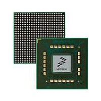
MPC8536DS Freescale Semiconductor, MPC8536DS Datasheet - Page 1679

MPC8536DS
Manufacturer Part Number
MPC8536DS
Description
BOARD DEV SYSTEM MPC8536E
Manufacturer
Freescale Semiconductor
Series
PowerQUICC III™r
Type
MPUr
Datasheets
1.MPC8536EBVTAVLA.pdf
(127 pages)
2.MPC8536EBVTAVLA.pdf
(1706 pages)
3.MPC8536DS.pdf
(2 pages)
4.MPC8536DS.pdf
(126 pages)
Specifications of MPC8536DS
Contents
Board, Software and Documentation
Processor Series
MPC85xx
Core
e500
Data Bus Width
32 bit
Maximum Clock Frequency
667 MHz
Operating Supply Voltage
- 0.3 V to + 1.21 V
Maximum Operating Temperature
+ 105 C
Data Ram Size
32 KB
Interface Type
SPI, USB
Program Memory Type
DDR2, DDR3, SDRAM
Core Size
32 Bit
Program Memory Size
544KB
Cpu Speed
1.5GHz
Digital Ic Case Style
BGA
No. Of Pins
783
Supply Voltage Range
0.95V To 1.05V
Rohs Compliant
Yes
For Use With/related Products
MPC8536
Lead Free Status / RoHS Status
Lead free / RoHS Compliant
- MPC8536EBVTAVLA PDF datasheet
- MPC8536EBVTAVLA PDF datasheet #2
- MPC8536DS PDF datasheet #3
- MPC8536DS PDF datasheet #4
- Current page: 1679 of 1706
- Download datasheet (15Mb)
D
E
F
G
H
I
Freescale Semiconductor
Direct-mapped cache. A cache in which each main memory address can appear in only
Double data rate. Memory that allows data transfers at the start and end of a clock cycle.
Effective address (EA). The 32-bit address specified for a load, store, or an instruction
Exclusive state. MEI state (E) in which only one caching device contains data that is also
Fetch. Retrieving instructions from either the cache or main memory and placing them
Flush. An operation that causes a cache block to be invalidated and the data, if modified,
Frame-check sequence (FCS). Specifies the standard 32-bit cyclic redundancy check
General-purpose register (GPR). Any of the 32 registers in the general-purpose register
Guarded. The guarded attribute pertains to out-of-order execution. When a page is
Harvard architecture. An architectural model featuring separate caches and other
Illegal instructions. A class of instructions that are not implemented for a particular
Implementation. A particular processor that conforms to the architecture, but may differ
MPC83536E PowerQUICC™ III Integrated Processor Reference Manual, Rev. 1
one location within the cache; operates more quickly when the memory request is
a cache hit.
thereby doubling the data rate.
fetch. This address is then submitted to the MMU for translation to either a
physical memory
in system memory.
into the instruction queue.
to be written to memory.
(CRC) obtained using the standard CCITT-CRC polynomial on all fields except
the preamble, SFD, and CRC.
file. These registers provide the source operands and destination results for all
integer data manipulation instructions. Integer load instructions move data from
memory to GPRs and store instructions move data from GPRs to memory.
designated as guarded, instructions and data cannot be accessed out-of-order.
memory management resources for instructions and data.
processor. These include instructions not defined by the architecture. In addition,
for 32-bit implementations, instructions that are defined only for 64-bit
implementations are considered to be illegal instructions. For 64-bit
implementations instructions that are defined only for 32-bit implementations are
considered to be illegal instructions.
from other architecture-compliant implementations for example in design, feature
set, and implementation of optional features.
address or an I/O address.
Glossary-3
Related parts for MPC8536DS
Image
Part Number
Description
Manufacturer
Datasheet
Request
R
Part Number:
Description:
Manufacturer:
Freescale Semiconductor, Inc
Datasheet:
Part Number:
Description:
Manufacturer:
Freescale Semiconductor, Inc
Datasheet:
Part Number:
Description:
Manufacturer:
Freescale Semiconductor, Inc
Datasheet:
Part Number:
Description:
Manufacturer:
Freescale Semiconductor, Inc
Datasheet:
Part Number:
Description:
Manufacturer:
Freescale Semiconductor, Inc
Datasheet:
Part Number:
Description:
Manufacturer:
Freescale Semiconductor, Inc
Datasheet:
Part Number:
Description:
Manufacturer:
Freescale Semiconductor, Inc
Datasheet:
Part Number:
Description:
Manufacturer:
Freescale Semiconductor, Inc
Datasheet:
Part Number:
Description:
Manufacturer:
Freescale Semiconductor, Inc
Datasheet:
Part Number:
Description:
Manufacturer:
Freescale Semiconductor, Inc
Datasheet:
Part Number:
Description:
Manufacturer:
Freescale Semiconductor, Inc
Datasheet:
Part Number:
Description:
Manufacturer:
Freescale Semiconductor, Inc
Datasheet:
Part Number:
Description:
Manufacturer:
Freescale Semiconductor, Inc
Datasheet:
Part Number:
Description:
Manufacturer:
Freescale Semiconductor, Inc
Datasheet:
Part Number:
Description:
Manufacturer:
Freescale Semiconductor, Inc
Datasheet:


