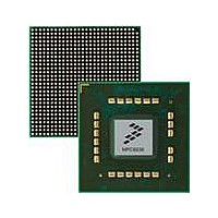
MPC8536DS Freescale Semiconductor, MPC8536DS Datasheet - Page 633

MPC8536DS
Manufacturer Part Number
MPC8536DS
Description
BOARD DEV SYSTEM MPC8536E
Manufacturer
Freescale Semiconductor
Series
PowerQUICC III™r
Type
MPUr
Datasheets
1.MPC8536EBVTAVLA.pdf
(127 pages)
2.MPC8536EBVTAVLA.pdf
(1706 pages)
3.MPC8536DS.pdf
(2 pages)
4.MPC8536DS.pdf
(126 pages)
Specifications of MPC8536DS
Contents
Board, Software and Documentation
Processor Series
MPC85xx
Core
e500
Data Bus Width
32 bit
Maximum Clock Frequency
667 MHz
Operating Supply Voltage
- 0.3 V to + 1.21 V
Maximum Operating Temperature
+ 105 C
Data Ram Size
32 KB
Interface Type
SPI, USB
Program Memory Type
DDR2, DDR3, SDRAM
Core Size
32 Bit
Program Memory Size
544KB
Cpu Speed
1.5GHz
Digital Ic Case Style
BGA
No. Of Pins
783
Supply Voltage Range
0.95V To 1.05V
Rohs Compliant
Yes
For Use With/related Products
MPC8536
Lead Free Status / RoHS Status
Lead free / RoHS Compliant
- MPC8536EBVTAVLA PDF datasheet
- MPC8536EBVTAVLA PDF datasheet #2
- MPC8536DS PDF datasheet #3
- MPC8536DS PDF datasheet #4
- Current page: 633 of 1706
- Download datasheet (15Mb)
12.3.1.10
The ULSRs are read-only registers that monitor the status of the data transfer on the UART buses. To
isolate the status bits from the proper character received through the UART bus, software should read the
ULSR and then the URBR.
Figure 12-12
Table 12-16
Freescale Semiconductor
Bits Name
0
1
2
3
4
TEMT Transmitter empty.
THRE Transmitter holding register empty.
RFE Receiver FIFO error.
Offset UART0: 0x505, UART1: 0x605
FE
Reset
BI
W
R
0 This bit is cleared when there are no errors in the receiver FIFO or on a read of the ULSR with no remaining
1 Set to one when one of the characters in the receiver FIFO encounters an error (framing, parity, or break
0 Either or both the UTHR or the internal transmitter shift register has a data character. In FIFO mode, a data
1 Both the UTHR and the internal transmitter shift register are empty. In FIFO mode, both the transmitter FIFO
0 The UTHR is not empty.
1 A data character has transferred from the UTHR into the internal transmitter shift register. In FIFO mode, the
Break interrupt.
0 This bit is cleared when the ULSR is read or when a valid data transfer is detected (that is, STOP bit is received).
1 Received data of logic 0 for more than START bit + Data bits + Parity bit + one STOP bits length of time. A new
Framing error.
0 This bit is cleared when ULSR is read or when a new character is loaded into the URBR from the receiver shift
1 Invalid STOP bit for receive data (only the first STOP bit is checked). In FIFO mode, this bit is set when the
describes the fields of the ULSRs.
shows the bits in the ULSRs.
receiver FIFO errors.
interrupt)
character is in the transmitter FIFO or the internal transmitter shift register.
and the internal transmitter shift register are empty.
transmitter FIFO contains no data character.
character is not loaded until SIN returns to the mark state (logic 1) and a valid START is detected. In FIFO mode,
a zero character is encountered in the FIFO (the zero character is at the top of the FIFO). In FIFO mode, only
one zero character is stored.
register.
character that detected a framing error is encountered in the FIFO (that is the character at the top of the FIFO).
An attempt to resynchronize occurs after a framing error. The UART assumes that the framing error (due to a
logic 0 being read when a logic 1 (STOP) was expected) was due to a STOP bit overlapping with the next START
bit, so it assumes this logic 0 sample is a true START bit and then receives the following new data.
Line Status Registers (ULSR n )
RFE
0
0
MPC8536E PowerQUICC III Integrated Processor Reference Manual, Rev. 1
TEMT
1
1
Figure 12-12. Line Status Register (ULSR)
Table 12-16. ULSR Field Descriptions
THRE
1
2
BI
0
3
Description
FE
0
4
PE
0
5
OE
0
6
Access: Read only
DR
0
7
DUART
12-15
Related parts for MPC8536DS
Image
Part Number
Description
Manufacturer
Datasheet
Request
R
Part Number:
Description:
Manufacturer:
Freescale Semiconductor, Inc
Datasheet:
Part Number:
Description:
Manufacturer:
Freescale Semiconductor, Inc
Datasheet:
Part Number:
Description:
Manufacturer:
Freescale Semiconductor, Inc
Datasheet:
Part Number:
Description:
Manufacturer:
Freescale Semiconductor, Inc
Datasheet:
Part Number:
Description:
Manufacturer:
Freescale Semiconductor, Inc
Datasheet:
Part Number:
Description:
Manufacturer:
Freescale Semiconductor, Inc
Datasheet:
Part Number:
Description:
Manufacturer:
Freescale Semiconductor, Inc
Datasheet:
Part Number:
Description:
Manufacturer:
Freescale Semiconductor, Inc
Datasheet:
Part Number:
Description:
Manufacturer:
Freescale Semiconductor, Inc
Datasheet:
Part Number:
Description:
Manufacturer:
Freescale Semiconductor, Inc
Datasheet:
Part Number:
Description:
Manufacturer:
Freescale Semiconductor, Inc
Datasheet:
Part Number:
Description:
Manufacturer:
Freescale Semiconductor, Inc
Datasheet:
Part Number:
Description:
Manufacturer:
Freescale Semiconductor, Inc
Datasheet:
Part Number:
Description:
Manufacturer:
Freescale Semiconductor, Inc
Datasheet:
Part Number:
Description:
Manufacturer:
Freescale Semiconductor, Inc
Datasheet:


