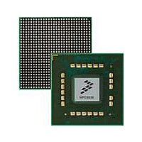
MPC8536DS Freescale Semiconductor, MPC8536DS Datasheet - Page 1588

MPC8536DS
Manufacturer Part Number
MPC8536DS
Description
BOARD DEV SYSTEM MPC8536E
Manufacturer
Freescale Semiconductor
Series
PowerQUICC III™r
Type
MPUr
Datasheets
1.MPC8536EBVTAVLA.pdf
(127 pages)
2.MPC8536EBVTAVLA.pdf
(1706 pages)
3.MPC8536DS.pdf
(2 pages)
4.MPC8536DS.pdf
(126 pages)
Specifications of MPC8536DS
Contents
Board, Software and Documentation
Processor Series
MPC85xx
Core
e500
Data Bus Width
32 bit
Maximum Clock Frequency
667 MHz
Operating Supply Voltage
- 0.3 V to + 1.21 V
Maximum Operating Temperature
+ 105 C
Data Ram Size
32 KB
Interface Type
SPI, USB
Program Memory Type
DDR2, DDR3, SDRAM
Core Size
32 Bit
Program Memory Size
544KB
Cpu Speed
1.5GHz
Digital Ic Case Style
BGA
No. Of Pins
783
Supply Voltage Range
0.95V To 1.05V
Rohs Compliant
Yes
For Use With/related Products
MPC8536
Lead Free Status / RoHS Status
Lead free / RoHS Compliant
- MPC8536EBVTAVLA PDF datasheet
- MPC8536EBVTAVLA PDF datasheet #2
- MPC8536DS PDF datasheet #3
- MPC8536DS PDF datasheet #4
- Current page: 1588 of 1706
- Download datasheet (15Mb)
1
Debug Features and Watchpoint Facility
25.2.2
This section describes the details of the debug, watchpoint monitor, and JTAG test signals
25.2.2.1
Table 25-3
25-6
While these signals are normally bidirectional, when sourcing debug information they are output only.
THERM[0:1]
L1_TSTCLK
L2_TSTCLK
TEST_SEL
LSSD_
MODE
Name
TRST
TDO
TMS
MDVAL
Signal
TDI
describes all signals associated with device debug modes.
Detailed Signal Descriptions
Debug Signals—Details
Description
Test select 1
Test mode
Test reset
Test data
Test data
Thermal
I/O
resistor
access
O Memory data-valid. Indicates when valid data is available. May be used by a logic analyzer to
output
select
input
Table 25-2. Debug, Watchpoint and Test Signal Summary (continued)
Test
Test
Test
MPC8536E PowerQUICC III Integrated Processor Reference Manual, Rev. 1
capture the data on the data bus.
Meaning
Table 25-3. Debug Signals—Detailed Signal Descriptions
Timing Asserted/Negated—Referenced to the selected interface, (DDR or local bus).
State
Functional
Debug
Debug
Debug
Debug
Block
Asserted—Indicates that data is valid on the data bus during the current clock cycle.
Test
Test
Test
Test
Test
When the DDR SDRAM interface is selected to source information on MDVAL,
this signal is valid for every cycle that data is driven or received on the DDR
SDRAM interface. When the LBC is selected, this signal is valid for every cycle
that data is driven or received on the local bus interface. The assertion of this
signal may be used by a logic analyzer to capture data.
Asserts when data is valid. Assertions are held for the duration of the transfer.
Read data timing is similar to MA. Write data timing is similar to the output
MDQ.
Serial input for instructions and data to the JTAG test
subsystem. Internally pulled up.
Serial data output for the JTAG test subsystem. High
impedance except when scanning out data.
Carries commands to the TAP controller for boundary scan
operations. Internally pulled up.
Resets the TAP controller asynchronously.
These pins tie directly to an internal resistor whose value
varies linearly with temperature.
Factory test. Must be negated (pulled high) for normal
operation.
Factory Test. Refer to the MPC8536E Integrated Processor
Hardware Specifications for proper treatment.
Factory Test. Refer to the MPC8536E Integrated Processor
Hardware Specifications for proper treatment.
Factory Test. Refer to the MPC8536E Integrated Processor
Hardware Specifications for proper treatment.
Description
Function
Freescale Semiconductor
Reset
Value
Hi Z
—
—
—
1
1
I/O Page #
O
I
I
I
I
I
I
I
I
25-8
25-8
25-8
25-8
25-8
25-8
25-8
25-8
25-8
Related parts for MPC8536DS
Image
Part Number
Description
Manufacturer
Datasheet
Request
R
Part Number:
Description:
Manufacturer:
Freescale Semiconductor, Inc
Datasheet:
Part Number:
Description:
Manufacturer:
Freescale Semiconductor, Inc
Datasheet:
Part Number:
Description:
Manufacturer:
Freescale Semiconductor, Inc
Datasheet:
Part Number:
Description:
Manufacturer:
Freescale Semiconductor, Inc
Datasheet:
Part Number:
Description:
Manufacturer:
Freescale Semiconductor, Inc
Datasheet:
Part Number:
Description:
Manufacturer:
Freescale Semiconductor, Inc
Datasheet:
Part Number:
Description:
Manufacturer:
Freescale Semiconductor, Inc
Datasheet:
Part Number:
Description:
Manufacturer:
Freescale Semiconductor, Inc
Datasheet:
Part Number:
Description:
Manufacturer:
Freescale Semiconductor, Inc
Datasheet:
Part Number:
Description:
Manufacturer:
Freescale Semiconductor, Inc
Datasheet:
Part Number:
Description:
Manufacturer:
Freescale Semiconductor, Inc
Datasheet:
Part Number:
Description:
Manufacturer:
Freescale Semiconductor, Inc
Datasheet:
Part Number:
Description:
Manufacturer:
Freescale Semiconductor, Inc
Datasheet:
Part Number:
Description:
Manufacturer:
Freescale Semiconductor, Inc
Datasheet:
Part Number:
Description:
Manufacturer:
Freescale Semiconductor, Inc
Datasheet:


