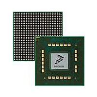
MPC8536DS Freescale Semiconductor, MPC8536DS Datasheet - Page 1607

MPC8536DS
Manufacturer Part Number
MPC8536DS
Description
BOARD DEV SYSTEM MPC8536E
Manufacturer
Freescale Semiconductor
Series
PowerQUICC III™r
Type
MPUr
Datasheets
1.MPC8536EBVTAVLA.pdf
(127 pages)
2.MPC8536EBVTAVLA.pdf
(1706 pages)
3.MPC8536DS.pdf
(2 pages)
4.MPC8536DS.pdf
(126 pages)
Specifications of MPC8536DS
Contents
Board, Software and Documentation
Processor Series
MPC85xx
Core
e500
Data Bus Width
32 bit
Maximum Clock Frequency
667 MHz
Operating Supply Voltage
- 0.3 V to + 1.21 V
Maximum Operating Temperature
+ 105 C
Data Ram Size
32 KB
Interface Type
SPI, USB
Program Memory Type
DDR2, DDR3, SDRAM
Core Size
32 Bit
Program Memory Size
544KB
Cpu Speed
1.5GHz
Digital Ic Case Style
BGA
No. Of Pins
783
Supply Voltage Range
0.95V To 1.05V
Rohs Compliant
Yes
For Use With/related Products
MPC8536
Lead Free Status / RoHS Status
Lead free / RoHS Compliant
- MPC8536EBVTAVLA PDF datasheet
- MPC8536EBVTAVLA PDF datasheet #2
- MPC8536DS PDF datasheet #3
- MPC8536DS PDF datasheet #4
- Current page: 1607 of 1706
- Download datasheet (15Mb)
25.4.2
The DDR interface has two debug modes distinguished by which pins drive the debug information. In one
mode, debug information (source ID, data valid) is multiplexed onto the ECC pins; the other mode uses
the debug pins.
25.4.2.1
If MSRCID0 is high when sampled during POR, the debug information from the DDR SDRAM interface
is driven on MSRCID[0:4] and MDVAL. This POR value is captured in PORDBGMSR[MEM_SEL] as
described in
source ID appears on MSRCID[0:4] during a RAS or CAS cycle. During any other cycle, the value of
MSRCID[0:4] is all ones, which indicates idle cycles on the address/command interface. Similarly,
MDVAL is asserted during valid data cycles on the DDR interface.
25.4.2.2
If MSRCID1 is low when sampled during POR, debug information from the DDR SDRAM interface is
selected to appear on MECC[0:5] as shown in
(the source ID), appears on MECC[0:4] during a RAS or CAS cycle. During any other cycle the value of
MECC[0:4] is all ones. A data-valid signal (DVAL) is driven on MECC5 during valid DDR SDRAM data
cycles.
Freescale Semiconductor
Value
(Hex)
0A
0B
0C
0D
0E
06
07
08
09
0F
DDR SDRAM Interface Debug
Section 23.4.1.5, “POR Debug Mode Status Register (PORDBGMSR).”
Debug Information on Debug Pins
Debug Information on ECC Pins
Reserved
Security
SATA2/Configuration space
USB3
Boot sequencer
eSDHC
Reserved
SATA1
Reserved
Local space (DDR)
In this mode, MECC[0:5] must be disconnected from all SDRAM devices
to prevent contention on those lines.
MPC8536E PowerQUICC III Integrated Processor Reference Manual, Rev. 1
Source (or Target) Port
Table 25-26. Source and Target ID Values (continued)
Figure
NOTE
Value
(Hex)
25-1. In this mode, the ID value of the source port,
1A
1B
1C
1D
1E
16
17
18
19
1F
Reserved
System access port (SAP)
eTSEC1
Reserved
eTSEC3
Reserved
Reserved
Reserved
Reserved
Non-valid port indicator (reserved for debug
info)
Source (or Target) Port
Debug Features and Watchpoint Facility
In this mode, the
25-25
Related parts for MPC8536DS
Image
Part Number
Description
Manufacturer
Datasheet
Request
R
Part Number:
Description:
Manufacturer:
Freescale Semiconductor, Inc
Datasheet:
Part Number:
Description:
Manufacturer:
Freescale Semiconductor, Inc
Datasheet:
Part Number:
Description:
Manufacturer:
Freescale Semiconductor, Inc
Datasheet:
Part Number:
Description:
Manufacturer:
Freescale Semiconductor, Inc
Datasheet:
Part Number:
Description:
Manufacturer:
Freescale Semiconductor, Inc
Datasheet:
Part Number:
Description:
Manufacturer:
Freescale Semiconductor, Inc
Datasheet:
Part Number:
Description:
Manufacturer:
Freescale Semiconductor, Inc
Datasheet:
Part Number:
Description:
Manufacturer:
Freescale Semiconductor, Inc
Datasheet:
Part Number:
Description:
Manufacturer:
Freescale Semiconductor, Inc
Datasheet:
Part Number:
Description:
Manufacturer:
Freescale Semiconductor, Inc
Datasheet:
Part Number:
Description:
Manufacturer:
Freescale Semiconductor, Inc
Datasheet:
Part Number:
Description:
Manufacturer:
Freescale Semiconductor, Inc
Datasheet:
Part Number:
Description:
Manufacturer:
Freescale Semiconductor, Inc
Datasheet:
Part Number:
Description:
Manufacturer:
Freescale Semiconductor, Inc
Datasheet:
Part Number:
Description:
Manufacturer:
Freescale Semiconductor, Inc
Datasheet:


