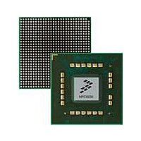
MPC8536DS Freescale Semiconductor, MPC8536DS Datasheet - Page 1506

MPC8536DS
Manufacturer Part Number
MPC8536DS
Description
BOARD DEV SYSTEM MPC8536E
Manufacturer
Freescale Semiconductor
Series
PowerQUICC III™r
Type
MPUr
Datasheets
1.MPC8536EBVTAVLA.pdf
(127 pages)
2.MPC8536EBVTAVLA.pdf
(1706 pages)
3.MPC8536DS.pdf
(2 pages)
4.MPC8536DS.pdf
(126 pages)
Specifications of MPC8536DS
Contents
Board, Software and Documentation
Processor Series
MPC85xx
Core
e500
Data Bus Width
32 bit
Maximum Clock Frequency
667 MHz
Operating Supply Voltage
- 0.3 V to + 1.21 V
Maximum Operating Temperature
+ 105 C
Data Ram Size
32 KB
Interface Type
SPI, USB
Program Memory Type
DDR2, DDR3, SDRAM
Core Size
32 Bit
Program Memory Size
544KB
Cpu Speed
1.5GHz
Digital Ic Case Style
BGA
No. Of Pins
783
Supply Voltage Range
0.95V To 1.05V
Rohs Compliant
Yes
For Use With/related Products
MPC8536
Lead Free Status / RoHS Status
Lead free / RoHS Compliant
- MPC8536EBVTAVLA PDF datasheet
- MPC8536EBVTAVLA PDF datasheet #2
- MPC8536DS PDF datasheet #3
- MPC8536DS PDF datasheet #4
- Current page: 1506 of 1706
- Download datasheet (15Mb)
Global Utilities
Table 23-10
23.4.1.8
GENCFGR is shown in
Table 23-11
23.4.1.9
Shown in
alternate functions on GPIO, on local bus chip select pins LCS[5:7], and interrupt input pins IRQ[9:11],
respectively. Specifically, DMA request, acknowledge, and done signals comprise the secondary functions
for the associated IRQ and local bus chip select signals.
It contains also the SPI/ eSDHC, GPIO/eSDHC, GPIO/USB1, GPIO/USB2 and GPIO/PCI controls for
pinmux.
23-14
0–31 POR_CFG_VEC General-purpose POR configuration vector sampled from local bus address/data signals at the
Bits
Offset 0x030
3–31
Reset
Bits
0–1
2
W
R
0
—
Figure
Name
SDHC_WP_INV
1
describes the bit settings of GENCFGR.
describes the bit settings of GPPORCR.
General Configuration Register (GENCFGR)
Alternate Function Signal Multiplex Control Register (PMUXCR)
SDHC_WP_INV
Name
—
—
23-9, PMUXCR contains bits that enable DMA channels 0, 1, 2 and 3 which exist as
MPC8536E PowerQUICC III Integrated Processor Reference Manual, Rev. 1
2
negation of HRESET. Note that if nothing is driven on these signals during reset, the value of this
register is indeterminate.
Figure
Figure 23-8. General Configuration Register (GENCFGR)
Reserved
Secure digital WP polarity
0 SDHC_WP is active high (0=write enabled, 1=write protected).
1 SDHC_WP is active low (0=write protected, 1=write enabled).
Note: This bit should be set to 1 if PMUXCR[SDHC_WP]=0 (SDHC_WP not exposed to pins)
Reserved
3
and eSDHC write functionality is required.
23-8.
Table 23-10. GPPORCR Field Descriptions
Table 23-11. GENCFGR Field Descriptions
All zeros
Description
Description
—
Freescale Semiconductor
Access: Read Only
31
Related parts for MPC8536DS
Image
Part Number
Description
Manufacturer
Datasheet
Request
R
Part Number:
Description:
Manufacturer:
Freescale Semiconductor, Inc
Datasheet:
Part Number:
Description:
Manufacturer:
Freescale Semiconductor, Inc
Datasheet:
Part Number:
Description:
Manufacturer:
Freescale Semiconductor, Inc
Datasheet:
Part Number:
Description:
Manufacturer:
Freescale Semiconductor, Inc
Datasheet:
Part Number:
Description:
Manufacturer:
Freescale Semiconductor, Inc
Datasheet:
Part Number:
Description:
Manufacturer:
Freescale Semiconductor, Inc
Datasheet:
Part Number:
Description:
Manufacturer:
Freescale Semiconductor, Inc
Datasheet:
Part Number:
Description:
Manufacturer:
Freescale Semiconductor, Inc
Datasheet:
Part Number:
Description:
Manufacturer:
Freescale Semiconductor, Inc
Datasheet:
Part Number:
Description:
Manufacturer:
Freescale Semiconductor, Inc
Datasheet:
Part Number:
Description:
Manufacturer:
Freescale Semiconductor, Inc
Datasheet:
Part Number:
Description:
Manufacturer:
Freescale Semiconductor, Inc
Datasheet:
Part Number:
Description:
Manufacturer:
Freescale Semiconductor, Inc
Datasheet:
Part Number:
Description:
Manufacturer:
Freescale Semiconductor, Inc
Datasheet:
Part Number:
Description:
Manufacturer:
Freescale Semiconductor, Inc
Datasheet:


