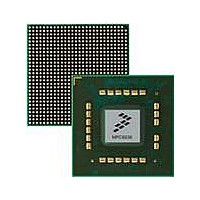
MPC8536DS Freescale Semiconductor, MPC8536DS Datasheet - Page 252

MPC8536DS
Manufacturer Part Number
MPC8536DS
Description
BOARD DEV SYSTEM MPC8536E
Manufacturer
Freescale Semiconductor
Series
PowerQUICC III™r
Type
MPUr
Datasheets
1.MPC8536EBVTAVLA.pdf
(127 pages)
2.MPC8536EBVTAVLA.pdf
(1706 pages)
3.MPC8536DS.pdf
(2 pages)
4.MPC8536DS.pdf
(126 pages)
Specifications of MPC8536DS
Contents
Board, Software and Documentation
Processor Series
MPC85xx
Core
e500
Data Bus Width
32 bit
Maximum Clock Frequency
667 MHz
Operating Supply Voltage
- 0.3 V to + 1.21 V
Maximum Operating Temperature
+ 105 C
Data Ram Size
32 KB
Interface Type
SPI, USB
Program Memory Type
DDR2, DDR3, SDRAM
Core Size
32 Bit
Program Memory Size
544KB
Cpu Speed
1.5GHz
Digital Ic Case Style
BGA
No. Of Pins
783
Supply Voltage Range
0.95V To 1.05V
Rohs Compliant
Yes
For Use With/related Products
MPC8536
Lead Free Status / RoHS Status
Lead free / RoHS Compliant
- MPC8536EBVTAVLA PDF datasheet
- MPC8536EBVTAVLA PDF datasheet #2
- MPC8536DS PDF datasheet #3
- MPC8536DS PDF datasheet #4
- Current page: 252 of 1706
- Download datasheet (15Mb)
L2 Look-Aside Cache/SRAM
6.8.1
PLRU bit updates depend on which cache way was last accessed, as summarized in
When an L2 line is invalidated, the PLRU bits are updated, marking the corresponding way as
least-recently used. This causes the invalidated way to be selected as the next victim.
6.8.2
The general PLRU algorithm described above must be modified to take into account special features of
the L2 cache; namely SRAM regions, line locking, and stash-only regions. Each of these features reserves
ways within each cache set such that some ways are not eligible for allocation/victimization by the general
LRU algorithm.
To preserve the state of the ways that are set aside for other special functions, the PLRU pointers are
modified by a mask that is a function of the L2 configuration registers, the lock bits in the cache status
array, and initiator of the transaction. The mask effectively points the PLRU algorithm away from ways
that are not to be considered for replacement.
L2 cache lines are locked through the status array lock bits. There are two lock bits for each way of each
set (1024 sets by eight ways). These bits are set or cleared through special L2 controller commands.There
are two sets of lock bits, one for instructions (I0–I7) and one for data (D0–D7) for every line. The lock bits
act as a mask over the PLRU bits to determine victim selection. The PLRU bits are updated regardless of
line locking.
Lock bits are used at allocate time to steer the PLRU algorithm away from selecting locked victims. In the
following discussion, the eight lock bits for a particular set are called L0–L7.
An effective value of each PLRU bit is calculated as follows:
6-32
Where Lock Way i: Li = Di | Ii, i=0…7 (Di = data lock, Ii = instruction lock)
P0_eff = f(P0,L0,L1,L2,L3,L4,L5,L6,L7) = (L0 & L1 & L2 & L3) | (P0 & ~(L4 & L5 & L6 & L7))
P1_eff = f(P1,L0,L1,L2,L3) = (L0 & L1) | (P1 & ~(L2 & L3))
P2_eff = f(P2,L4,L5,L6,L7) = (L4 & L5) | (P2 & ~(L6 & L7))
PLRU Bit Update Considerations
Allocation of Lines
MPC8536E PowerQUICC III Integrated Processor Reference Manual, Rev. 1
Table 6-24. PLRU Bit Update Algorithm
Accessed
Last Way
0
1
2
3
4
5
6
7
P0 P1 P2 P3 P4 P5 P6
1
1
1
1
0
0
0
0
—
—
—
—
1
1
0
0
—
—
—
—
PLRU Bits
1
1
0
0
—
—
—
—
—
—
1
0
—
—
—
—
—
—
1
0
—
—
—
—
—
—
1
0
—
—
—
—
—
—
1
0
Freescale Semiconductor
Table
6-24.
Related parts for MPC8536DS
Image
Part Number
Description
Manufacturer
Datasheet
Request
R
Part Number:
Description:
Manufacturer:
Freescale Semiconductor, Inc
Datasheet:
Part Number:
Description:
Manufacturer:
Freescale Semiconductor, Inc
Datasheet:
Part Number:
Description:
Manufacturer:
Freescale Semiconductor, Inc
Datasheet:
Part Number:
Description:
Manufacturer:
Freescale Semiconductor, Inc
Datasheet:
Part Number:
Description:
Manufacturer:
Freescale Semiconductor, Inc
Datasheet:
Part Number:
Description:
Manufacturer:
Freescale Semiconductor, Inc
Datasheet:
Part Number:
Description:
Manufacturer:
Freescale Semiconductor, Inc
Datasheet:
Part Number:
Description:
Manufacturer:
Freescale Semiconductor, Inc
Datasheet:
Part Number:
Description:
Manufacturer:
Freescale Semiconductor, Inc
Datasheet:
Part Number:
Description:
Manufacturer:
Freescale Semiconductor, Inc
Datasheet:
Part Number:
Description:
Manufacturer:
Freescale Semiconductor, Inc
Datasheet:
Part Number:
Description:
Manufacturer:
Freescale Semiconductor, Inc
Datasheet:
Part Number:
Description:
Manufacturer:
Freescale Semiconductor, Inc
Datasheet:
Part Number:
Description:
Manufacturer:
Freescale Semiconductor, Inc
Datasheet:
Part Number:
Description:
Manufacturer:
Freescale Semiconductor, Inc
Datasheet:


