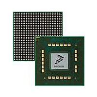
MPC8536DS Freescale Semiconductor, MPC8536DS Datasheet - Page 727

MPC8536DS
Manufacturer Part Number
MPC8536DS
Description
BOARD DEV SYSTEM MPC8536E
Manufacturer
Freescale Semiconductor
Series
PowerQUICC III™r
Type
MPUr
Datasheets
1.MPC8536EBVTAVLA.pdf
(127 pages)
2.MPC8536EBVTAVLA.pdf
(1706 pages)
3.MPC8536DS.pdf
(2 pages)
4.MPC8536DS.pdf
(126 pages)
Specifications of MPC8536DS
Contents
Board, Software and Documentation
Processor Series
MPC85xx
Core
e500
Data Bus Width
32 bit
Maximum Clock Frequency
667 MHz
Operating Supply Voltage
- 0.3 V to + 1.21 V
Maximum Operating Temperature
+ 105 C
Data Ram Size
32 KB
Interface Type
SPI, USB
Program Memory Type
DDR2, DDR3, SDRAM
Core Size
32 Bit
Program Memory Size
544KB
Cpu Speed
1.5GHz
Digital Ic Case Style
BGA
No. Of Pins
783
Supply Voltage Range
0.95V To 1.05V
Rohs Compliant
Yes
For Use With/related Products
MPC8536
Lead Free Status / RoHS Status
Lead free / RoHS Compliant
- MPC8536EBVTAVLA PDF datasheet
- MPC8536EBVTAVLA PDF datasheet #2
- MPC8536DS PDF datasheet #3
- MPC8536DS PDF datasheet #4
- Current page: 727 of 1706
- Download datasheet (15Mb)
The uppermost byte select (LBS0), when asserted, indicates that LAD[0:7] contains valid data during a
cycle. Likewise, LBS1 indicates that LAD[8:15] contain valid data, LBS2 indicates that LAD[16:23]
contains valid data, and LBS3 indicates that LAD[24:31] contain valid data. For a UPM refresh timer
request, all LBS[0:3] signals are asserted/negated by the UPM according to the refresh pattern only.
Following any internal bus monitor exception, the LBS[0:3] signals are negated regardless of the
exception handling provided by any UPM exception pattern to prevent spurious writes to external RAM.
13.4.4.4.4
The general-purpose signals (LGPL[0:5]) each have two bits in the RAM word that define the logical value
of the signal to be changed at the rising edge of the bus clock and/or at the falling edge of the bus clock.
LGPL0 offers enhancements beyond the other LGPLn lines.
LGPL0 can be controlled by an address line specified in MxMR[G0CL]. To use this feature, G0H and G0L
should be set in the RAM word. For example, for a SIMM with multiple banks, this address line can be
used to switch between internal memory device banks.
13.4.4.4.5
The LOOP bit in the RAM word specifies the beginning and end of a set of UPM RAM words that are to
be repeated. The first time LOOP = 1, the memory controller recognizes it as a loop start word and loads
the memory loop counter with the corresponding contents of the loop field shown in
RAM word for which LOOP = 1 is recognized as a loop end word. When it is reached, the loop counter is
decremented by one.
Continued loop execution depends on the loop counter. If the counter is not zero, the next RAM word
executed is the loop start word. Otherwise, the next RAM word executed is the one after the loop end word.
Loops can be executed sequentially but cannot be nested. Also, special care must be taken:
Freescale Semiconductor
•
•
LAST and LOOP must not be set together.
Loop start word should not have an AMX change with regard to the previous word.
General-Purpose Signals (G n T n , GO n )
Loop Control (LOOP)
MPC8536E PowerQUICC III Integrated Processor Reference Manual, Rev. 1
UPMC
UPMA
UPMB
Figure 13-68. LBS Signal Selection
BR n [MSEL]
MUX
Bank Selected
BR n [PS]
Byte-Select
Byte count
Logic
LA[23:25]
Enhanced Local Bus Controller
Table
LBS0
LBS1
LBS2
LBS3
13-41. The next
13-85
Related parts for MPC8536DS
Image
Part Number
Description
Manufacturer
Datasheet
Request
R
Part Number:
Description:
Manufacturer:
Freescale Semiconductor, Inc
Datasheet:
Part Number:
Description:
Manufacturer:
Freescale Semiconductor, Inc
Datasheet:
Part Number:
Description:
Manufacturer:
Freescale Semiconductor, Inc
Datasheet:
Part Number:
Description:
Manufacturer:
Freescale Semiconductor, Inc
Datasheet:
Part Number:
Description:
Manufacturer:
Freescale Semiconductor, Inc
Datasheet:
Part Number:
Description:
Manufacturer:
Freescale Semiconductor, Inc
Datasheet:
Part Number:
Description:
Manufacturer:
Freescale Semiconductor, Inc
Datasheet:
Part Number:
Description:
Manufacturer:
Freescale Semiconductor, Inc
Datasheet:
Part Number:
Description:
Manufacturer:
Freescale Semiconductor, Inc
Datasheet:
Part Number:
Description:
Manufacturer:
Freescale Semiconductor, Inc
Datasheet:
Part Number:
Description:
Manufacturer:
Freescale Semiconductor, Inc
Datasheet:
Part Number:
Description:
Manufacturer:
Freescale Semiconductor, Inc
Datasheet:
Part Number:
Description:
Manufacturer:
Freescale Semiconductor, Inc
Datasheet:
Part Number:
Description:
Manufacturer:
Freescale Semiconductor, Inc
Datasheet:
Part Number:
Description:
Manufacturer:
Freescale Semiconductor, Inc
Datasheet:


