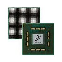
MPC8536DS Freescale Semiconductor, MPC8536DS Datasheet - Page 294

MPC8536DS
Manufacturer Part Number
MPC8536DS
Description
BOARD DEV SYSTEM MPC8536E
Manufacturer
Freescale Semiconductor
Series
PowerQUICC III™r
Type
MPUr
Datasheets
1.MPC8536EBVTAVLA.pdf
(127 pages)
2.MPC8536EBVTAVLA.pdf
(1706 pages)
3.MPC8536DS.pdf
(2 pages)
4.MPC8536DS.pdf
(126 pages)
Specifications of MPC8536DS
Contents
Board, Software and Documentation
Processor Series
MPC85xx
Core
e500
Data Bus Width
32 bit
Maximum Clock Frequency
667 MHz
Operating Supply Voltage
- 0.3 V to + 1.21 V
Maximum Operating Temperature
+ 105 C
Data Ram Size
32 KB
Interface Type
SPI, USB
Program Memory Type
DDR2, DDR3, SDRAM
Core Size
32 Bit
Program Memory Size
544KB
Cpu Speed
1.5GHz
Digital Ic Case Style
BGA
No. Of Pins
783
Supply Voltage Range
0.95V To 1.05V
Rohs Compliant
Yes
For Use With/related Products
MPC8536
Lead Free Status / RoHS Status
Lead free / RoHS Compliant
- MPC8536EBVTAVLA PDF datasheet
- MPC8536EBVTAVLA PDF datasheet #2
- MPC8536DS PDF datasheet #3
- MPC8536DS PDF datasheet #4
- Current page: 294 of 1706
- Download datasheet (15Mb)
DDR Memory Controller
Table 8-11
8-20
12–15
8–11
Bits
0–3
4–7
PRETOACT Precharge-to-activate interval (t
ACTTOPRE Activate to precharge interval (t
ACTTORW Activate to read/write interval for SDRAM (t
CASLAT
Name
describes TIMING_CFG_1 fields.
until an activate or refresh command is allowed.
0000 Reserved
0001 1 clock
0010 2 clocks
0011 3 clocks
0100 4 clocks
0101 5 clocks
0110 6 clocks
0111 7 clocks
until a precharge command is allowed. This field is concatenated with TIMING_CFG_3[EXT_ACTTOPRE]
to obtain a 5-bit value for the total activate to precharge time. Note that the decode of 0000–0011 is equal
to 16-19 clocks when TIMING_CFG_3[EXT_ACTTOPRE] = 0, but it is equal to 0-3 clocks when
TIMING_CFG_3[EXT_ACTTOPRE] = 1.
0000 16 clocks
0001 17 clocks
0010 18 clocks
0011 19 clocks
0100 4 clocks
command until a read or write command is allowed.
0000 Reserved
0001 1 clock
0010 2 clocks
0011 3 clocks
0100 4 clocks
0101 5 clocks
0110 6 clocks
0111 7 clocks
MCAS latency from READ command. Number of clock cycles between registration of a READ command
by the SDRAM and the availability of the first output data. If a READ command is registered at clock edge
n
concatenated with TIMING_CFG_3[EXT_CASLAT] to obtain a 5-bit value for the total CAS latency. This
value must be programmed at initialization as described in
Configuration 2
0000 Reserved
0001 1 clock
0010 1.5 clocks
0011 2 clocks
0100 2.5 clocks
0101 3 clocks
0110 3.5 clocks
0111 4 clocks
and the latency is
MPC8536E PowerQUICC III Integrated Processor Reference Manual, Rev. 1
Table 8-11. TIMING_CFG_1 Field Descriptions
(DDR_SDRAM_CFG_2).”)
m
clocks, data is available nominally coincident with clock edge
1000 8 clocks
1001 9 clocks
1010 10 clocks
1011 11 clocks
1100 12 clocks
1101 13 clocks
1110 14 clocks
1111 15 clocks
RAS
0101 5 clocks
0110 6 clocks
0111 7 clocks
…
1111 15 clocks
1000 8 clocks
1001 9 clocks
1010 10 clocks
1011 11 clocks
1100 12 clocks
1101 13 clocks
1110 14 clocks
1111 15 clocks
1000 4.5 clocks
1001 5 clocks
1010 5.5 clocks
1011 6 clocks
1100 6.5 clocks
1101 7 clocks
1110 7.5 clocks
1111 8 clocks
RP
). Determines the number of clock cycles from a precharge command
). Determines the number of clock cycles from an activate command
RCD
Description
). Controls the number of clock cycles from an activate
Section 8.4.1.9, “DDR SDRAM Control
Freescale Semiconductor
n
+
m
. This field is
Related parts for MPC8536DS
Image
Part Number
Description
Manufacturer
Datasheet
Request
R
Part Number:
Description:
Manufacturer:
Freescale Semiconductor, Inc
Datasheet:
Part Number:
Description:
Manufacturer:
Freescale Semiconductor, Inc
Datasheet:
Part Number:
Description:
Manufacturer:
Freescale Semiconductor, Inc
Datasheet:
Part Number:
Description:
Manufacturer:
Freescale Semiconductor, Inc
Datasheet:
Part Number:
Description:
Manufacturer:
Freescale Semiconductor, Inc
Datasheet:
Part Number:
Description:
Manufacturer:
Freescale Semiconductor, Inc
Datasheet:
Part Number:
Description:
Manufacturer:
Freescale Semiconductor, Inc
Datasheet:
Part Number:
Description:
Manufacturer:
Freescale Semiconductor, Inc
Datasheet:
Part Number:
Description:
Manufacturer:
Freescale Semiconductor, Inc
Datasheet:
Part Number:
Description:
Manufacturer:
Freescale Semiconductor, Inc
Datasheet:
Part Number:
Description:
Manufacturer:
Freescale Semiconductor, Inc
Datasheet:
Part Number:
Description:
Manufacturer:
Freescale Semiconductor, Inc
Datasheet:
Part Number:
Description:
Manufacturer:
Freescale Semiconductor, Inc
Datasheet:
Part Number:
Description:
Manufacturer:
Freescale Semiconductor, Inc
Datasheet:
Part Number:
Description:
Manufacturer:
Freescale Semiconductor, Inc
Datasheet:


