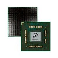
MPC8536DS Freescale Semiconductor, MPC8536DS Datasheet - Page 299

MPC8536DS
Manufacturer Part Number
MPC8536DS
Description
BOARD DEV SYSTEM MPC8536E
Manufacturer
Freescale Semiconductor
Series
PowerQUICC III™r
Type
MPUr
Datasheets
1.MPC8536EBVTAVLA.pdf
(127 pages)
2.MPC8536EBVTAVLA.pdf
(1706 pages)
3.MPC8536DS.pdf
(2 pages)
4.MPC8536DS.pdf
(126 pages)
Specifications of MPC8536DS
Contents
Board, Software and Documentation
Processor Series
MPC85xx
Core
e500
Data Bus Width
32 bit
Maximum Clock Frequency
667 MHz
Operating Supply Voltage
- 0.3 V to + 1.21 V
Maximum Operating Temperature
+ 105 C
Data Ram Size
32 KB
Interface Type
SPI, USB
Program Memory Type
DDR2, DDR3, SDRAM
Core Size
32 Bit
Program Memory Size
544KB
Cpu Speed
1.5GHz
Digital Ic Case Style
BGA
No. Of Pins
783
Supply Voltage Range
0.95V To 1.05V
Rohs Compliant
Yes
For Use With/related Products
MPC8536
Lead Free Status / RoHS Status
Lead free / RoHS Compliant
- MPC8536EBVTAVLA PDF datasheet
- MPC8536EBVTAVLA PDF datasheet #2
- MPC8536DS PDF datasheet #3
- MPC8536DS PDF datasheet #4
- Current page: 299 of 1706
- Download datasheet (15Mb)
Freescale Semiconductor
17–23
24–25
Bits
14
15
16
26
27
28
29
BA_INTLV_CTL
x32_EN
PCHB8
3T_EN
2T_EN
NCAP
Name
HSE
—
—
MPC8536E PowerQUICC III Integrated Processor Reference Manual, Rev. 1
Table 8-13. DDR_SDRAM_CFG Field Descriptions (continued)
precharge. If one of these devices is used, then this bit needs to be set if auto precharge is used.
0 DRAMs in system support concurrent auto-precharge.
1 DRAMs in system do not support concurrent auto-precharge.
Enable 3T timing. This field cannot be set if DDR_SDRAM_CFG[2T_EN] is also set. This field cannot
be used with a 32-bit bus if 4-beat bursts are used.
0 1T timing is enabled if 2T_EN is cleared. The DRAM command/address are held for only 1 cycle
1 3T timing is enabled. The DRAM command/address are held for 3 full cycles on the DRAM bus
Enable 2T timing.This field should not be set if DDR_SDrAM_CFG[3T_EN] is set.
0 1T timing is enabled if 3T_EN is cleared. The DRAM command/address are held for only 1 cycle
1 2T timing is enabled. The DRAM command/address are held for 2 full cycles on the DRAM bus
Note: RD_EN and 2T_EN must not both be set at the same time.
(‘ x ’ denotes a don’t care bit value. All unlisted field values are reserved.)
0000000 No external memory banks are interleaved
1000000 External memory banks 0 and 1 are interleaved
0100000 External memory banks 2 and 3 are interleaved
1100000 External memory banks 0 and 1 are interleaved together and
xx 00100 External memory banks 0 through 3 are all interleaved together
Reserved
0 Either x8 or x16 discrete DRAM chips are used. In this mode, each data byte has a dedicated
1 x32 discrete DRAM chips are used. In this mode, DQS0 is used to capture DQ[0:31], DQS4 is
0 MA[10] is used to indicate the auto-precharge and precharge all commands.
1 MA[8] is used to indicate the auto-precharge and precharge all commands.
If x32_EN is cleared, then PCHB8 should be cleared as well.
Sets I/O driver impedance to half strength. This impedance is used by the MDIC, address/command,
data, and clock impedance values, but only if automatic hardware calibration is disabled and the
corresponding group's software override is disabled in the DDR control driver register(s) described
in
using automatic hardware calibration.
0 I/O driver impedance is configured to full strength.
1 I/O driver impedance is configured to half strength.
Reserved
Non-concurrent auto-precharge. Some older DDR DRAMs do not support concurrent auto
Bank (chip select) interleaving control. Set this field only if you wish to use bank interleaving.
x32 enable.
Precharge bit 8 enable.
Global half-strength override
Section 8.4.1.27, “DDR Control Driver Register 1
on the DRAM bus.
for every DRAM transaction. However, the chip select is only held for the third cycle.
on the DRAM bus.
for every DRAM transaction. However, the chip select is only held for the second cycle.
corresponding data strobe.
used to capture DQ[32:63] and DQS8 is used to capture ECC[0:7].
banks 2 and 3 are interleaved together
Description
S
(DDRCDR_1).” This bit should be cleared if
DDR Memory Controller
8-25
Related parts for MPC8536DS
Image
Part Number
Description
Manufacturer
Datasheet
Request
R
Part Number:
Description:
Manufacturer:
Freescale Semiconductor, Inc
Datasheet:
Part Number:
Description:
Manufacturer:
Freescale Semiconductor, Inc
Datasheet:
Part Number:
Description:
Manufacturer:
Freescale Semiconductor, Inc
Datasheet:
Part Number:
Description:
Manufacturer:
Freescale Semiconductor, Inc
Datasheet:
Part Number:
Description:
Manufacturer:
Freescale Semiconductor, Inc
Datasheet:
Part Number:
Description:
Manufacturer:
Freescale Semiconductor, Inc
Datasheet:
Part Number:
Description:
Manufacturer:
Freescale Semiconductor, Inc
Datasheet:
Part Number:
Description:
Manufacturer:
Freescale Semiconductor, Inc
Datasheet:
Part Number:
Description:
Manufacturer:
Freescale Semiconductor, Inc
Datasheet:
Part Number:
Description:
Manufacturer:
Freescale Semiconductor, Inc
Datasheet:
Part Number:
Description:
Manufacturer:
Freescale Semiconductor, Inc
Datasheet:
Part Number:
Description:
Manufacturer:
Freescale Semiconductor, Inc
Datasheet:
Part Number:
Description:
Manufacturer:
Freescale Semiconductor, Inc
Datasheet:
Part Number:
Description:
Manufacturer:
Freescale Semiconductor, Inc
Datasheet:
Part Number:
Description:
Manufacturer:
Freescale Semiconductor, Inc
Datasheet:


