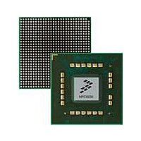
MPC8536DS Freescale Semiconductor, MPC8536DS Datasheet - Page 605

MPC8536DS
Manufacturer Part Number
MPC8536DS
Description
BOARD DEV SYSTEM MPC8536E
Manufacturer
Freescale Semiconductor
Series
PowerQUICC III™r
Type
MPUr
Datasheets
1.MPC8536EBVTAVLA.pdf
(127 pages)
2.MPC8536EBVTAVLA.pdf
(1706 pages)
3.MPC8536DS.pdf
(2 pages)
4.MPC8536DS.pdf
(126 pages)
Specifications of MPC8536DS
Contents
Board, Software and Documentation
Processor Series
MPC85xx
Core
e500
Data Bus Width
32 bit
Maximum Clock Frequency
667 MHz
Operating Supply Voltage
- 0.3 V to + 1.21 V
Maximum Operating Temperature
+ 105 C
Data Ram Size
32 KB
Interface Type
SPI, USB
Program Memory Type
DDR2, DDR3, SDRAM
Core Size
32 Bit
Program Memory Size
544KB
Cpu Speed
1.5GHz
Digital Ic Case Style
BGA
No. Of Pins
783
Supply Voltage Range
0.95V To 1.05V
Rohs Compliant
Yes
For Use With/related Products
MPC8536
Lead Free Status / RoHS Status
Lead free / RoHS Compliant
- MPC8536EBVTAVLA PDF datasheet
- MPC8536EBVTAVLA PDF datasheet #2
- MPC8536DS PDF datasheet #3
- MPC8536DS PDF datasheet #4
- Current page: 605 of 1706
- Download datasheet (15Mb)
The I
address is always zero; however the I
broadcast message is the master address. Because the second byte is automatically acknowledged by
hardware, the receiver device software must verify that the broadcast message is intended for itself by
reading the second byte of the message. If the master address is for another receiver device and the third
byte is a write command, software can ignore the third byte during the broadcast. If the master address is
for another receiver device and the third byte is a read command, software must write 0xFF to I2CDR with
I2CCR[TXAK] = 1, so that it does not interfere with the data written from the addressed device.
Each data byte is 8 bits long. Data bits can be changed only while SCL is low and must be held stable while
SCL is high, as shown in
significant bit (msb) is transmitted first. Each byte of data must be followed by an acknowledge bit, which
is signaled from the receiving device by pulling the SDA line low at the 9th clock. Therefore, one complete
data byte transfer takes 9 clock pulses. Several bytes can be transferred during a data transfer session.
If the slave receiver does not acknowledge the master, the SDA line must be left high by the slave. The
master can then generate a stop condition to abort the data transfer or a START condition (repeated
START) to begin a new calling.
If the master receiver does not acknowledge the slave transmitter after a byte of transmission, the slave
interprets that the end-of-data has been reached. Then the slave releases the SDA line for the master to
generate a STOP or a START condition.
11.4.1.3
Figure 11-8
terminate the previous transfer. The master uses this method to communicate with another slave or with
the same slave in a different mode (transmit/receive mode) without releasing the bus.
11.4.1.4
The master can terminate the transfer by generating a STOP condition to free the bus. A STOP condition
is defined as a low-to-high transition of the SDA signal while SCL is high. For more information, see
Figure
at which point the slave must release the bus. The STOP condition is initiated by a software write that
clears I2CCR[MSTA].
As described in
condition followed by a calling address without generating a STOP condition for the previous transfer.
This is called a repeated START condition.
11.4.1.5
The following sections give details of how aspects of the protocol are implemented in this I
Freescale Semiconductor
2
C module responds to a general call (broadcast) command when I2CCR[BCST] is set. A broadcast
11-8. Note that a master can generate a STOP even if the slave has transmitted an acknowledge bit,
shows a repeated START condition, which is generated without a STOP condition that can
Repeated START Condition
STOP Condition
Protocol Implementation Details
Section 11.4.1.3, “Repeated START Condition,”
MPC8536E PowerQUICC III Integrated Processor Reference Manual, Rev. 1
Figure
11-8. There is one clock pulse on SCL for each data bit, and the most
2
C module does not check the R/W bit. The second byte of the
the master can generate a START
2
C module.
I
2
C Interfaces
11-13
Related parts for MPC8536DS
Image
Part Number
Description
Manufacturer
Datasheet
Request
R
Part Number:
Description:
Manufacturer:
Freescale Semiconductor, Inc
Datasheet:
Part Number:
Description:
Manufacturer:
Freescale Semiconductor, Inc
Datasheet:
Part Number:
Description:
Manufacturer:
Freescale Semiconductor, Inc
Datasheet:
Part Number:
Description:
Manufacturer:
Freescale Semiconductor, Inc
Datasheet:
Part Number:
Description:
Manufacturer:
Freescale Semiconductor, Inc
Datasheet:
Part Number:
Description:
Manufacturer:
Freescale Semiconductor, Inc
Datasheet:
Part Number:
Description:
Manufacturer:
Freescale Semiconductor, Inc
Datasheet:
Part Number:
Description:
Manufacturer:
Freescale Semiconductor, Inc
Datasheet:
Part Number:
Description:
Manufacturer:
Freescale Semiconductor, Inc
Datasheet:
Part Number:
Description:
Manufacturer:
Freescale Semiconductor, Inc
Datasheet:
Part Number:
Description:
Manufacturer:
Freescale Semiconductor, Inc
Datasheet:
Part Number:
Description:
Manufacturer:
Freescale Semiconductor, Inc
Datasheet:
Part Number:
Description:
Manufacturer:
Freescale Semiconductor, Inc
Datasheet:
Part Number:
Description:
Manufacturer:
Freescale Semiconductor, Inc
Datasheet:
Part Number:
Description:
Manufacturer:
Freescale Semiconductor, Inc
Datasheet:


