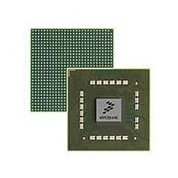
MPC8544VTALF Freescale Semiconductor, MPC8544VTALF Datasheet - Page 995

MPC8544VTALF
Manufacturer Part Number
MPC8544VTALF
Description
MPU POWERQUICC III 783-PBGA
Manufacturer
Freescale Semiconductor
Datasheets
1.MPC8544VTALF.pdf
(117 pages)
2.MPC8544VTALF.pdf
(2 pages)
3.MPC8544VTALF.pdf
(1340 pages)
Specifications of MPC8544VTALF
Processor Type
MPC85xx PowerQUICC III 32-Bit
Speed
667MHz
Voltage
1V
Mounting Type
Surface Mount
Package / Case
783-FCPBGA
Processor Series
MPC85xx
Core
e500
Data Bus Width
32 bit
Maximum Clock Frequency
667 MHz
Maximum Operating Temperature
+ 105 C
Mounting Style
SMD/SMT
Data Ram Size
32 KB
I/o Voltage
1.8 V, 3.3 V
Interface Type
I2C, HSSI, DUART
Minimum Operating Temperature
0 C
Lead Free Status / RoHS Status
Lead free / RoHS Compliant
Features
-
Lead Free Status / Rohs Status
Lead free / RoHS Compliant
Available stocks
Company
Part Number
Manufacturer
Quantity
Price
Company:
Part Number:
MPC8544VTALF
Manufacturer:
Freescale Semiconductor
Quantity:
10 000
Company:
Part Number:
MPC8544VTALFA
Manufacturer:
Freescale Semiconductor
Quantity:
10 000
- Current page: 995 of 1340
- Download datasheet (12Mb)
17.3
The PCI controller supports the following two types of registers:
17.3.1
The PCI memory mapped registers are accessed by reading and writing to an address comprised of the base
address (specified in the CCSRBAR on the local side or the PCSRBAR on the PCI side) plus the block
base address, plus the offset of the specific register to be accessed. Note that all memory-mapped registers
(except the PCI configuration data register, PCI CFG_DATA) must only be accessed as 32-bit quantities.
Table 17-3
In this table and in the register figures and field descriptions, the following access definitions apply:
Freescale Semiconductor
Offset
0x000
•
•
•
•
•
•
•
PCI_CLK
Signal
Memory-mapped registers—these registers control PCI address translation, PCI error
management, and PCI configuration register access. These registers are described in
Section 17.3.1, “PCI Memory-Mapped Registers,”
PCI configuration registers contained within the PCI configuration header—these registers are
specified by the PCI bus specification for every PCI device. These registers are described in
Section 17.3.2, “PCI Configuration Header,”
Reserved fields are always ignored for the purposes of determining access type.
R/W, R, and W (read/write, read only, and write only) indicate that all the non-reserved fields in a
register have the same access type.
w1c indicates that all of the non-reserved fields in a register are cleared by writing ones to them.
Mixed indicates a combination of access types.
Special is used when no other category applies. In this case the register figure and field description
table should be read carefully.
Memory Map/Register Definitions
CFG_ADDR—PCI configuration address
lists the memory-mapped registers.
PCI Memory-Mapped Registers
MPC8544E PowerQUICC III Integrated Host Processor Family Reference Manual, Rev. 1
Table 17-2. PCI Interface Signals—Detailed Signal Descriptions (continued)
I/O
I PCI clock is an independent clock that may be used for the PCI interface. If used the PCI operation is
PCI Controller Memory-Mapped Registers—Block Base Address 0x0_8000
asynchronous with respect to SYSCLK and the platform clock. In order to used this signal as the PCI
clock source, it must be designated during POR configuration. See the reset chapter for POR details
regarding clock selection as well as proper PCI frequency selection.
Timing Assertion/Negation—See the device Hardware Specification for specific timing information.
Table 17-3. PCI Memory-Mapped Register Map
Register
PCI Configuration Access Registers
and its subsections.
Description
and its subsections.
Access
R/W
0x0000_0000
Reset
17.3.1.1.1/17-14
PCI Bus Interface
Section/page
17-11
Related parts for MPC8544VTALF
Image
Part Number
Description
Manufacturer
Datasheet
Request
R
Part Number:
Description:
Manufacturer:
Freescale Semiconductor, Inc
Datasheet:
Part Number:
Description:
Manufacturer:
Freescale Semiconductor, Inc
Datasheet:
Part Number:
Description:
Manufacturer:
Freescale Semiconductor, Inc
Datasheet:
Part Number:
Description:
Manufacturer:
Freescale Semiconductor, Inc
Datasheet:
Part Number:
Description:
Manufacturer:
Freescale Semiconductor, Inc
Datasheet:
Part Number:
Description:
Manufacturer:
Freescale Semiconductor, Inc
Datasheet:
Part Number:
Description:
Manufacturer:
Freescale Semiconductor, Inc
Datasheet:
Part Number:
Description:
Manufacturer:
Freescale Semiconductor, Inc
Datasheet:
Part Number:
Description:
Manufacturer:
Freescale Semiconductor, Inc
Datasheet:
Part Number:
Description:
Manufacturer:
Freescale Semiconductor, Inc
Datasheet:
Part Number:
Description:
Manufacturer:
Freescale Semiconductor, Inc
Datasheet:
Part Number:
Description:
Manufacturer:
Freescale Semiconductor, Inc
Datasheet:
Part Number:
Description:
Manufacturer:
Freescale Semiconductor, Inc
Datasheet:
Part Number:
Description:
Manufacturer:
Freescale Semiconductor, Inc
Datasheet:
Part Number:
Description:
Manufacturer:
Freescale Semiconductor, Inc
Datasheet:


