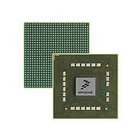
MPC8544VTALF Freescale Semiconductor, MPC8544VTALF Datasheet - Page 683

MPC8544VTALF
Manufacturer Part Number
MPC8544VTALF
Description
MPU POWERQUICC III 783-PBGA
Manufacturer
Freescale Semiconductor
Datasheets
1.MPC8544VTALF.pdf
(117 pages)
2.MPC8544VTALF.pdf
(2 pages)
3.MPC8544VTALF.pdf
(1340 pages)
Specifications of MPC8544VTALF
Processor Type
MPC85xx PowerQUICC III 32-Bit
Speed
667MHz
Voltage
1V
Mounting Type
Surface Mount
Package / Case
783-FCPBGA
Processor Series
MPC85xx
Core
e500
Data Bus Width
32 bit
Maximum Clock Frequency
667 MHz
Maximum Operating Temperature
+ 105 C
Mounting Style
SMD/SMT
Data Ram Size
32 KB
I/o Voltage
1.8 V, 3.3 V
Interface Type
I2C, HSSI, DUART
Minimum Operating Temperature
0 C
Lead Free Status / RoHS Status
Lead free / RoHS Compliant
Features
-
Lead Free Status / Rohs Status
Lead free / RoHS Compliant
Available stocks
Company
Part Number
Manufacturer
Quantity
Price
Company:
Part Number:
MPC8544VTALF
Manufacturer:
Freescale Semiconductor
Quantity:
10 000
Company:
Part Number:
MPC8544VTALFA
Manufacturer:
Freescale Semiconductor
Quantity:
10 000
- Current page: 683 of 1340
- Download datasheet (12Mb)
14.4.4.2.1
The following example further illustrates the steps required to perform two writes to the RAM array at
non-sequential addresses assuming that the relevant BRn and ORn registers have been previously setup.
Note that if step 1 (or 6) and 2 (or 7) are reversed, then step 3 (or 8) is replaced by the following:
14.4.4.2.2
RAM array contents may also be read for debug purposes, for example, by alternating dummy read
transactions, each time followed by reads of MDR (when MxMR[OP] = 0b10). The following example
further illustrates the steps required to perform two reads from the RAM array at non-sequential addresses
assuming that the relevant BRn and ORn registers have been previously setup.
Freescale Semiconductor
1. Program MxMR for the first write (with desired RAM array address).
2. Write pattern/data to MDR to ensure that the MxMR has already been updated with the desired
3. Read MDR to ensure that the MDR has already been updated with the desired pattern. (Or, read
4. Preform a dummy write transaction. (Write transaction can now be performed.)
5. Read/check MxMR[MAD]. If incremented, then the previous dummy write transaction is
6. Program MxMR for the second write with the desired RAM array address.
7. Write pattern/data to MDR to ensure that the MxMR has already been updated with the desired
8. Read MDR to ensure that the MDR has already been updated with the desired pattern.
9. Perform a dummy write transaction.(Write transaction can now be performed.)
10. Read/check MxMR[MAD]. If incremented, then the previous dummy write transaction is
•
1. Program MxMR for the first read with the desired RAM array address.
2. Read MxMR to ensure that the MxMR has already been updated with the desired configuration,
3. Perform a dummy read transaction.(Read transaction can now be performed.)
4. Read/check MxMR[MAD]. If incremented, then the previous dummy read transaction is
5. Read MDR.
6. Program MxMR for the second read with the desired RAM array address.
7. Read MxMR to ensure that the MxMR has already been updated with the desired configuration,
8. Perform a dummy read transaction.(Read transaction can now be performed.)
configuration.
MxMR if step 2 is not performed.)
completed; proceed to step 6. Repeat step 5 until incremented.
configuration.
completed.
Read MxMR to ensure that the MxMR has already been updated with the desired configuration.
such as RAM array address.
completed; proceed to step 5. Repeat step 4 until incremented.
such as RAM array address.
MPC8544E PowerQUICC III Integrated Host Processor Family Reference Manual, Rev. 1
UPM Programming Example (Two Sequential Writes to the
RAM Array)
RAM Array)
UPM Programming Example (Two Sequential Reads from the
Local Bus Controller
14-63
Related parts for MPC8544VTALF
Image
Part Number
Description
Manufacturer
Datasheet
Request
R
Part Number:
Description:
Manufacturer:
Freescale Semiconductor, Inc
Datasheet:
Part Number:
Description:
Manufacturer:
Freescale Semiconductor, Inc
Datasheet:
Part Number:
Description:
Manufacturer:
Freescale Semiconductor, Inc
Datasheet:
Part Number:
Description:
Manufacturer:
Freescale Semiconductor, Inc
Datasheet:
Part Number:
Description:
Manufacturer:
Freescale Semiconductor, Inc
Datasheet:
Part Number:
Description:
Manufacturer:
Freescale Semiconductor, Inc
Datasheet:
Part Number:
Description:
Manufacturer:
Freescale Semiconductor, Inc
Datasheet:
Part Number:
Description:
Manufacturer:
Freescale Semiconductor, Inc
Datasheet:
Part Number:
Description:
Manufacturer:
Freescale Semiconductor, Inc
Datasheet:
Part Number:
Description:
Manufacturer:
Freescale Semiconductor, Inc
Datasheet:
Part Number:
Description:
Manufacturer:
Freescale Semiconductor, Inc
Datasheet:
Part Number:
Description:
Manufacturer:
Freescale Semiconductor, Inc
Datasheet:
Part Number:
Description:
Manufacturer:
Freescale Semiconductor, Inc
Datasheet:
Part Number:
Description:
Manufacturer:
Freescale Semiconductor, Inc
Datasheet:
Part Number:
Description:
Manufacturer:
Freescale Semiconductor, Inc
Datasheet:


