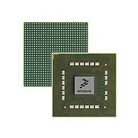
MPC8544VTALF Freescale Semiconductor, MPC8544VTALF Datasheet - Page 1238

MPC8544VTALF
Manufacturer Part Number
MPC8544VTALF
Description
MPU POWERQUICC III 783-PBGA
Manufacturer
Freescale Semiconductor
Datasheets
1.MPC8544VTALF.pdf
(117 pages)
2.MPC8544VTALF.pdf
(2 pages)
3.MPC8544VTALF.pdf
(1340 pages)
Specifications of MPC8544VTALF
Processor Type
MPC85xx PowerQUICC III 32-Bit
Speed
667MHz
Voltage
1V
Mounting Type
Surface Mount
Package / Case
783-FCPBGA
Processor Series
MPC85xx
Core
e500
Data Bus Width
32 bit
Maximum Clock Frequency
667 MHz
Maximum Operating Temperature
+ 105 C
Mounting Style
SMD/SMT
Data Ram Size
32 KB
I/o Voltage
1.8 V, 3.3 V
Interface Type
I2C, HSSI, DUART
Minimum Operating Temperature
0 C
Lead Free Status / RoHS Status
Lead free / RoHS Compliant
Features
-
Lead Free Status / Rohs Status
Lead free / RoHS Compliant
Available stocks
Company
Part Number
Manufacturer
Quantity
Price
Company:
Part Number:
MPC8544VTALF
Manufacturer:
Freescale Semiconductor
Quantity:
10 000
Company:
Part Number:
MPC8544VTALFA
Manufacturer:
Freescale Semiconductor
Quantity:
10 000
- Current page: 1238 of 1340
- Download datasheet (12Mb)
Debug Features and Watchpoint Facility
21.2.2.2
Table 21-4
21.2.2.3
Table 21-5
21-8
Signal
TCK
TDI
TRIG_OUT
TRIG_IN
Signal
shows detailed descriptions of the watchpoint monitor and trace buffer signals.
shows detailed descriptions of the JTAG test signals.
Watchpoint Monitor Trigger Signals—Details
Test Signals—Details
MPC8544E PowerQUICC III Integrated Host Processor Family Reference Manual, Rev. 1
I/O
I
I
Table 21-4. Watchpoint and Trigger Signals—Detailed Signal Descriptions
Table 21-5. JTAG Test and Other Signals—Detailed Signal Descriptions
I/O
JTAG test clock.
O Trigger out. Function determined by TOSR[SEL]. When TOSR[SEL] is non-zero, it can be used
JTAG test data input.
Meaning
I Trigger in. Can be used to trigger the watchpoint and trace buffers. Note this is an active-high
Meaning
Timing
State
Timing See IEEE 1149.1 standard for more details.
(rising-edge triggered) signal.
for triggering external devices, like a logic analyzer, with either the watchpoint monitor, the trace
buffer, or the performance monitor as trigger sources. When TOSR[SEL] is cleared, TRIG_OUT
is multiplexed with READY, which indicates the operational readiness of the device (running or in
low-power or debug modes). See
“Global Utilities,”
Meaning
Meaning
State
Timing Assertion/Negation—The MPC8544E interprets TRIG_IN as asserted on detection of
Timing Assertion may occur at any time. Remains asserted for at least 3 system clocks
State
State
Asserted/Negated—Should be driven by a free-running clock signal with a 30–70% duty cycle.
Asserted/Negated—The value present on the rising edge of TCK is clocked into the selected
See IEEE 1149.1 standard for more details.
Asserted—Indicates that a programmed/armed external event has been detected.
Asserted—When TOSR[SEL] is all zeros, serves as the READY signal, indicating that
Negation—No final watchpoint match condition
Input signals to the TAP are clocked in on the rising edge. Changes to the TAP output
signals occur on the falling edge. The test logic allows TCK to be stopped. An
unterminated input appears as a high signal level to the test logic due to an internal
pull-up resistor.
JTAG test instruction or data register. An unterminated input appears as a high signal
level to the test logic due to an internal pull-up resistor.
Assertion may be used internally to trigger trace buffers and watchpoint
mechanisms.
the rising edge. It may occur at any time. Must remain asserted for at least 3
system clocks to be recognized internally.
the device is not in a low-power or debug mode and that it has emerged from
reset. SEL ≠ 0 indicates that a programmed trigger event has occurred.
for more details about reset, low-power, and debug states.
Chapter 4, “Reset, Clocking, and Initialization,”
Description
Description
Freescale Semiconductor
and
Chapter 19,
Related parts for MPC8544VTALF
Image
Part Number
Description
Manufacturer
Datasheet
Request
R
Part Number:
Description:
Manufacturer:
Freescale Semiconductor, Inc
Datasheet:
Part Number:
Description:
Manufacturer:
Freescale Semiconductor, Inc
Datasheet:
Part Number:
Description:
Manufacturer:
Freescale Semiconductor, Inc
Datasheet:
Part Number:
Description:
Manufacturer:
Freescale Semiconductor, Inc
Datasheet:
Part Number:
Description:
Manufacturer:
Freescale Semiconductor, Inc
Datasheet:
Part Number:
Description:
Manufacturer:
Freescale Semiconductor, Inc
Datasheet:
Part Number:
Description:
Manufacturer:
Freescale Semiconductor, Inc
Datasheet:
Part Number:
Description:
Manufacturer:
Freescale Semiconductor, Inc
Datasheet:
Part Number:
Description:
Manufacturer:
Freescale Semiconductor, Inc
Datasheet:
Part Number:
Description:
Manufacturer:
Freescale Semiconductor, Inc
Datasheet:
Part Number:
Description:
Manufacturer:
Freescale Semiconductor, Inc
Datasheet:
Part Number:
Description:
Manufacturer:
Freescale Semiconductor, Inc
Datasheet:
Part Number:
Description:
Manufacturer:
Freescale Semiconductor, Inc
Datasheet:
Part Number:
Description:
Manufacturer:
Freescale Semiconductor, Inc
Datasheet:
Part Number:
Description:
Manufacturer:
Freescale Semiconductor, Inc
Datasheet:


